Spartan-3E FPGA Family: DC and Switching Characteristics
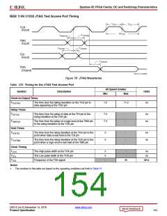
IEEE 1149.1/1532 JTAG Test Access Port Timing
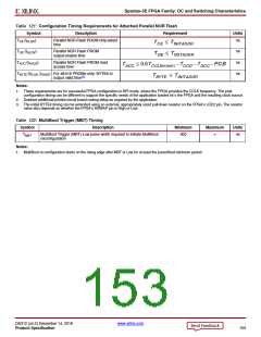
X-Ref Target - Figure 78
TCCH
TCCL
TCK
(Input)
1/FTCK
TTCKTMS
TTMSTCK
TMS
(Input)
TTDITCK
TTCKTDI
TDI
(Input)
TTCKTDO
TDO
(Output)
DS312-3_79_032409
Figure 78: JTAG Waveforms
Table 123: Timing for the JTAG Test Access Port
All Speed Grades
Min Max
Symbol
Description
Units
Clock-to-Output Times
TTCKTDO
The time from the falling transition on the TCK pin to
data appearing at the TDO pin
1.0
11.0
ns
Setup Times
TTDITCK
The time from the setup of data at the TDI pin to the
rising transition at the TCK pin
7.0
7.0
-
-
ns
ns
TTMSTCK
The time from the setup of a logic level at the TMS pin
to the rising transition at the TCK pin
Hold Times
TTCKTDI
The time from the rising transition at the TCK pin to the
point when data is last held at the TDI pin
0
0
-
-
ns
ns
TTCKTMS
The time from the rising transition at the TCK pin to the
point when a logic level is last held at the TMS pin
Clock Timing
TCCH
The High pulse width at the TCK pin
The Low pulse width at the TCK pin
Frequency of the TCK signal
5
5
-
-
-
ns
ns
TCCL
FTCK
30
MHz
Notes:
1. The numbers in this table are based on the operating conditions set forth in Table 77.
DS312 (v4.2) December 14, 2018
www.xilinx.com
Product Specification
154

 XILINX [ XILINX, INC ]