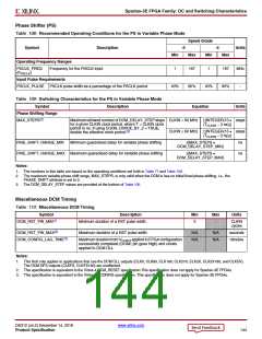
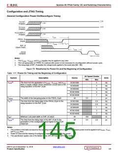
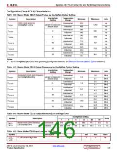
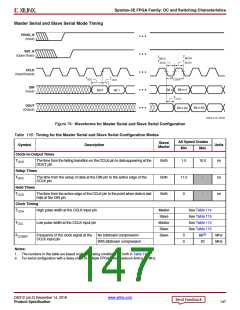
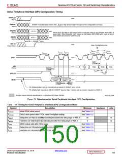
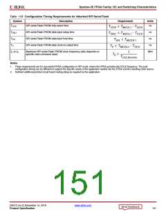
Spartan-3E FPGA Family: DC and Switching Characteristics
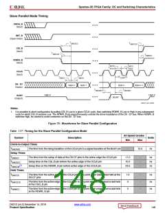
Slave Parallel Mode Timing
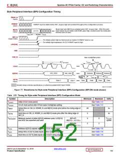
X-Ref Target
-
Figure 75
PROG_B
(Input)
INIT_B
(Open-Drain)
TSMCSCC
TSMCCCS
CSI_B
(Input)
TSMCCW
TSMWCC
RDWR_B
(Input)
TMCCH
TSCCH
TMCCL
TSCCL
CCLK
(Input)
1/FCCPAR
Byte n
TSMDCC
TSMCCD
D0 - D7
(Inputs)
Byte 0
Byte 1
Byte n+1
TSMCKBY
TSMCKBY
High-Z
High-Z
BUSY
(Output)
BUSY
DS312-3_02_103105
Notes:
1. It is possible to abort configuration by pulling CSI_B Low in a given CCLK cycle, then switching RDWR_B Low or High in any subsequent
cycle for which CSI_B remains Low. The RDWR_B pin asynchronously controls the driver impedance of the D0 - D7 bus. When RDWR_B
switches High, be careful to avoid contention on the D0 - D7 bus.
Figure 75: Waveforms for Slave Parallel Configuration
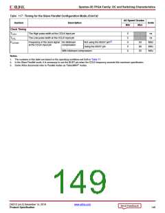
Table 117: Timing for the Slave Parallel Configuration Mode
All Speed Grades
Symbol
Description
Units
Min
Max
Clock-to-Output Times
TSMCKBY
The time from the rising transition on the CCLK pin to a signal transition at the BUSY pin
-
12.0
ns
Setup Times
TSMDCC
The time from the setup of data at the D0-D7 pins to the active edge the CCLK pin
Setup time on the CSI_B pin before the active edge of the CCLK pin
Setup time on the RDWR_B pin before active edge of the CCLK pin
11.0
10.0
23.0
-
-
-
ns
ns
ns
TSMCSCC
(2)
TSMCCW
Hold Times
TSMCCD
The time from the active edge of the CCLK pin to the point when data is last held at the
D0-D7 pins
1.0
0
-
-
-
ns
ns
ns
TSMCCCS
TSMWCC
The time from the active edge of the CCLK pin to the point when a logic level is last held
at the CSO_B pin
The time from the active edge of the CCLK pin to the point when a logic level is last held
at the RDWR_B pin
0
DS312 (v4.2) December 14, 2018
www.xilinx.com
Product Specification
148

 XILINX [ XILINX, INC ]