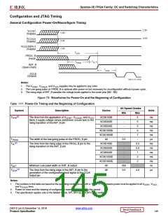
Spartan-3E FPGA Family: DC and Switching Characteristics
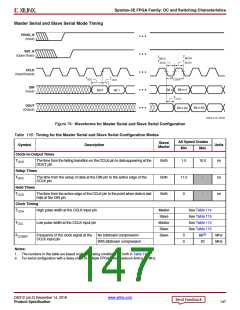
Master Serial and Slave Serial Mode Timing
X-Ref Target - Figure 74
PROG_B
(Input)
INIT_B
(Open-Drain)
TMCCH
TSCCH
TMCCL
TSCCL
CCLK
(Input/Output)
TDCC
1/FCCSER
TCCD
DIN
(Input)
Bit n+1
TCCO
Bit n
Bit 0
Bit 1
DOUT
(Output)
Bit n-63
Bit n-64
DS312-3_05_103105
Figure 74: Waveforms for Master Serial and Slave Serial Configuration
Table 116: Timing for the Master Serial and Slave Serial Configuration Modes
All Speed Grades
Slave/
Master
Symbol
Description
Units
Min
Max
Clock-to-Output Times
TCCO
The time from the falling transition on the CCLK pin to data appearing at the
DOUT pin
Both
Both
Both
1.5
10.0
ns
Setup Times
TDCC
The time from the setup of data at the DIN pin to the active edge of the
CCLK pin
11.0
0
-
-
ns
ns
Hold Times
TCCD
The time from the active edge of the CCLK pin to the point when data is last
held at the DIN pin
Clock Timing
TCCH
High pulse width at the CCLK input pin
Master
Slave
Master
Slave
Slave
See Table 114
See Table 115
See Table 114
See Table 115
66(2)
TCCL
Low pulse width at the CCLK input pin
FCCSER
Frequency of the clock signal at the
CCLK input pin
No bitstream compression
With bitstream compression
0
0
MHz
MHz
20
Notes:
1. The numbers in this table are based on the operating conditions set forth in Table 77.
2. For serial configuration with a daisy-chain of multiple FPGAs, the maximum limit is 25 MHz.
DS312 (v4.2) December 14, 2018
www.xilinx.com
Product Specification
147

 XILINX [ XILINX, INC ]