Spartan-3E FPGA Family: DC and Switching Characteristics
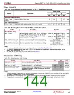
Phase Shifter (PS)
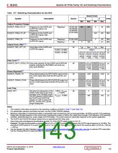
Table 108: Recommended Operating Conditions for the PS in Variable Phase Mode
Speed Grade
Symbol
Description
-5
-4
Units
Min
Max
Min
Max
Operating Frequency Ranges
PSCLK_FREQ
(FPSCLK
Frequency for the PSCLK input
1
167
1
167
MHz
-
)
Input Pulse Requirements
PSCLK_PULSE PSCLK pulse width as a percentage of the PSCLK period
40%
60%
40%
60%
Table 109: Switching Characteristics for the PS in Variable Phase Mode
Symbol
Phase Shifting Range
MAX_STEPS(2)
Description
Equation
Units
Maximum allowed number of DCM_DELAY_STEP steps CLKIN < 60 MHz
for a given CLKIN clock period, where T = CLKIN clock
[INTEGER(10 • steps
(TCLKIN – 3 ns))]
period in ns. If using CLKIN_DIVIDE_BY_2 = TRUE,
double the effective clock period.(3)
CLKIN ≥ 60 MHz
[INTEGER(15 • steps
(TCLKIN – 3 ns))]
FINE_SHIFT_RANGE_MIN
Minimum guaranteed delay for variable phase shifting
[MAX_STEPS •
DCM_DELAY_STEP_MIN]
ns
ns
FINE_SHIFT_RANGE_MAX Maximum guaranteed delay for variable phase shifting
[MAX_STEPS •
DCM_DELAY_STEP_MAX]
Notes:
1. The numbers in this table are based on the operating conditions set forth in Table 77 and Table 108.
2. The maximum variable phase shift range, MAX_STEPS, is only valid when the DCM is has no initial fixed phase shifting, i.e., the
PHASE_SHIFT attribute is set to 0.
3. The DCM_DELAY_STEP values are provided at the bottom of Table 105.
Miscellaneous DCM Timing
Table 110: Miscellaneous DCM Timing
Symbol
Description
Min
Max
Units
DCM_RST_PW_MIN(1)
Minimum duration of a RST pulse width
3
-
CLKIN
cycles
DCM_RST_PW_MAX(2)
Maximum duration of a RST pulse width
N/A
N/A
N/A
N/A
seconds
minutes
DCM_CONFIG_LAG_TIME(3)
Maximum duration from VCCINT applied to FPGA configuration
successfully completed (DONE pin goes High) and clocks
applied to DCM DLL
Notes:
1. This limit only applies to applications that use the DCM DLL outputs (CLK0, CLK90, CLK180, CLK270, CLK2X, CLK2X180, and CLKDV).
The DCM DFS outputs (CLKFX, CLKFX180) are unaffected.
2. This specification is equivalent to the Virtex-4 DCM_RESET specfication.This specification does not apply for Spartan-3E FPGAs.
3. This specification is equivalent to the Virtex-4 TCONFIG specification. This specification does not apply for Spartan-3E FPGAs.
DS312 (v4.2) December 14, 2018
www.xilinx.com
Product Specification
144

 XILINX [ XILINX, INC ]