Spartan-3E FPGA Family: DC and Switching Characteristics
Configuration and JTAG Timing
General Configuration Power-On/Reconfigure Timing
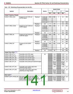
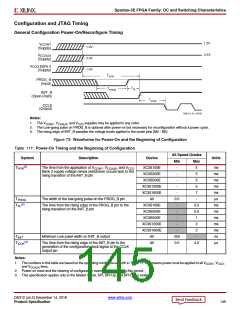
X-Ref Target - Figure 73
1.2V
2.5V
V
CCINT
1.0V
2.0V
1.0V
(Supply)
V
CCAUX
(Supply)
V
Bank 2
(Supply)
CCO
TPOR
PROG_B
(Input)
TPL
TPROG
INIT_B
(Open-Drain)
TICCK
CCLK
(Output)
DS312-3_01_103105
Notes:
1. The V
, V
, and V
supplies may be applied in any order.
CCINT
CCAUX
CCO
2. The Low-going pulse on PROG_B is optional after power-on but necessary for reconfiguration without a power cycle.
3. The rising edge of INIT_B samples the voltage levels applied to the mode pins (M0 - M2).
Figure 73: Waveforms for Power-On and the Beginning of Configuration
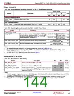
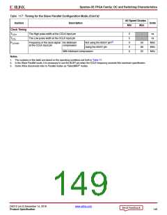
Table 111: Power-On Timing and the Beginning of Configuration
All Speed Grades
Symbol
Description
Device
Units
Min
Max
5
(2)
TPOR
The time from the application of VCCINT, VCCAUX, and VCCO
Bank 2 supply voltage ramps (whichever occurs last) to the
rising transition of the INIT_B pin
XC3S100E
XC3S250E
XC3S500E
XC3S1200E
XC3S1600E
All
-
ms
ms
ms
ms
ms
μs
-
5
-
5
-
5
-
7
TPROG
The width of the low-going pulse on the PROG_B pin
0.5
-
(2)
TPL
The time from the rising edge of the PROG_B pin to the
rising transition on the INIT_B pin
XC3S100E
XC3S250E
XC3S500E
XC3S1200E
XC3S1600E
All
-
0.5
0.5
1
ms
ms
ms
ms
ms
ns
-
-
-
2
-
2
TINIT
Minimum Low pulse width on INIT_B output
250
0.5
-
(3)
TICCK
The time from the rising edge of the INIT_B pin to the
generation of the configuration clock signal at the CCLK
output pin
All
4.0
μs
Notes:
1. The numbers in this table are based on the operating conditions set forth in Table 77. This means power must be applied to all V
, V
,
CCINT CCO
and V
lines.
CCAUX
2. Power-on reset and the clearing of configuration memory occurs during this period.
3. This specification applies only to the Master Serial, SPI, BPI-Up, and BPI-Down modes.
DS312 (v4.2) December 14, 2018
www.xilinx.com
Product Specification
145

 XILINX [ XILINX, INC ]