Spartan-3E FPGA Family: DC and Switching Characteristics
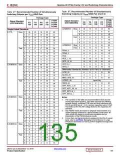
Table 97: Recommended Number of Simultaneously
Table 97: Recommended Number of Simultaneously
Switching Outputs per V
/GND Pair (Cont’d)
Switching Outputs per V
/GND Pair
CCO
CCO
Package Type
Package Type
FT256
FG320
FG400
FG484
FT256
FG320
FG400
FG484
Signal Standard
(IOSTANDARD)
Signal Standard
(IOSTANDARD)
VQ
100
TQ
144
PQ
208
CP
132
VQ
100
TQ
144
PQ
208
CP
132
LVCMOS15 Slow
2
4
6
2
4
6
2
2
16
8
10
7
10
7
19
9
55
31
18
25
16
13
55
31
16
13
11
17
16
15
18
Single-Ended Standards
LVTTL
Slow
2
4
34
20
10
10
6
19
10
7
52
26
26
13
13
6
60
41
29
22
13
11
34
20
15
12
10
9
6
5
5
9
17
17
8
Fast
9
9
9
13
7
6
7
7
7
8
6
5
5
5
5
12
16
2
8
6
5
LVCMOS12 Slow
Fast
17
10
8
11
10
8
11
10
8
16
10
16
13
11
16
16
15
18
5
5
5
Fast
17
9
17
9
17
9
26
13
13
6
PCI33_3
4
PCI66_3
8
8
8
6
7
7
7
PCIX
7
7
7
8
6
6
6
HSTL_I_18
HSTL_III_18
SSTL18_I
SSTL2_I
10
10
9
10
10
9
10
10
9
12
16
2
5
5
5
6
5
5
5
5
LVCMOS33 Slow
34
17
17
8
20
10
10
6
20
10
7
52
26
26
13
13
6
76
46
27
20
13
10
44
26
16
12
10
8
12
12
12
4
Differential Standards (Number of I/O Pairs or Channels)
6
LVDS_25
6
4
6
6
4
6
6
4
6
12
4
20
4
8
6
BLVDS_25
12
16
2
8
6
5
MINI_LVDS_25
LVPECL_25
12
20
5
5
5
Input Only
Fast
17
8
17
8
17
8
26
13
13
6
RSDS_25
6
5
5
4
6
6
5
5
4
6
6
5
5
4
6
12
20
8
4
DIFF_HSTL_I_18
DIFF_HSTL_IIII_18
DIFF_SSTL18_I
DIFF_SSTL2_I
8
8
7
9
6
8
6
6
8
8
6
6
6
7
12
16
2
5
5
5
6
8
8
8
5
5
LVCMOS25 Slow
28
13
13
6
16
10
7
16
10
7
42
19
19
9
76
46
33
24
18
42
20
15
13
11
64
34
22
18
36
21
13
10
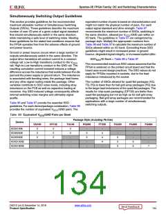
Notes:
4
1. The numbers in this table are recommendations that assume
sound board layout practice. This table assumes the following
parasitic factors: combined PCB trace and land inductance per
VCCO and GND pin of 1.0 nH, receiver capacitive load of 15 pF.
Test limits are the VIL/VIH voltage limits for the respective I/O
standard.
2. The PQ208 results are based on physical measurements of a
PQ208 package soldered to a typical printed circuit board. All
other results are based on worst-case simulation and an
interpolation of the PQ208 physical results.
6
8
6
6
12
2
6
6
6
9
Fast
17
9
16
9
16
9
26
13
13
6
4
6
9
7
7
3. If more than one signal standard is assigned to the I/Os of a given
bank, refer to XAPP689: Managing Ground Bounce in Large
FPGAs for information on how to perform weighted average SSO
calculations.
8
6
6
6
12
2
5
5
5
6
LVCMOS18 Slow
19
13
6
11
7
8
29
19
9
4
6
6
5
5
8
6
4
4
9
Fast
2
13
8
8
8
19
13
6
4
5
5
6
4
4
4
8
4
4
4
6
DS312 (v4.2) December 14, 2018
www.xilinx.com
Product Specification
135

 XILINX [ XILINX, INC ]