Spartan-3E FPGA Family: DC and Switching Characteristics
Simultaneously Switching Output Guidelines
This section provides guidelines for the recommended
maximum allowable number of Simultaneous Switching
Outputs (SSOs). These guidelines describe the maximum
number of user I/O pins of a given output signal standard
that should simultaneously switch in the same direction,
while maintaining a safe level of switching noise. Meeting
these guidelines for the stated test conditions ensures that
the FPGA operates free from the adverse effects of ground
and power bounce.
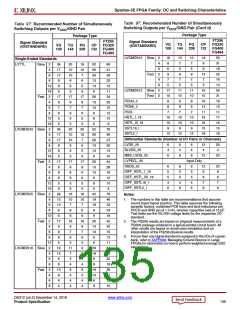
equivalent number of pairs is based on characterization and
might not match the physical number of pairs. For each
output signal standard and drive strength, Table 97
recommends the maximum number of SSOs, switching in
the same direction, allowed per V
/GND pair within an
CCO
I/O bank. The guidelines in Table 97 are categorized by
package style. Multiply the appropriate numbers from
Table 96 and Table 97 to calculate the maximum number of
SSOs allowed within an I/O bank. Exceeding these SSO
guidelines might result in increased power or ground
bounce, degraded signal integrity, or increased system jitter.
Ground or power bounce occurs when a large number of
outputs simultaneously switch in the same direction. The
output drive transistors all conduct current to a common
SSO
/IO Bank = Table 96 x Table 97
MAX
voltage rail. Low-to-High transitions conduct to the V
CCO
The recommended maximum SSO values assumes that the
FPGA is soldered on the printed circuit board and that the
board uses sound design practices. The SSO values do not
apply for FPGAs mounted in sockets, due to the lead
inductance introduced by the socket.
rail; High-to-Low transitions conduct to the GND rail. The
resulting cumulative current transient induces a voltage
difference across the inductance that exists between the die
pad and the power supply or ground return. The inductance
is associated with bonding wires, the package lead frame,
and any other signal routing inside the package. Other
variables contribute to SSO noise levels, including stray
inductance on the PCB as well as capacitive loading at
receivers. Any SSO-induced voltage consequently affects
internal switching noise margins and ultimately signal
quality.
The number of SSOs allowed for quad-flat packages (VQ,
TQ, PQ) is lower than for ball grid array packages (FG) due
to the larger lead inductance of the quad-flat packages. The
results for chip-scale packaging (CP132) are better than
quad-flat packaging but not as high as for ball grid array
packaging. Ball grid array packages are recommended for
applications with a large number of simultaneously
switching outputs.
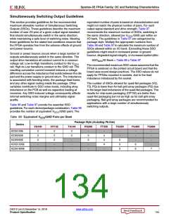
Table 96 and Table 97 provide the essential SSO
guidelines. For each device/package combination, Table 96
provides the number of equivalent V
/GND pairs. The
CCO
Table 96: Equivalent V
/GND Pairs per Bank
CCO
Package Style (including Pb-free)
Device
VQ100
CP132
TQ144
PQ208
FT256
FG320
FG400
FG484
XC3S100E
XC3S250E
XC3S500E
XC3S1200E
XC3S1600E
2
2
2
-
2
2
2
-
2
2
-
-
3
3
-
-
4
4
4
-
-
-
-
-
-
-
5
5
5
-
-
-
6
6
-
-
-
-
-
7
DS312 (v4.2) December 14, 2018
www.xilinx.com
Product Specification
134

 XILINX [ XILINX, INC ]