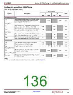
Spartan-3E FPGA Family: DC and Switching Characteristics
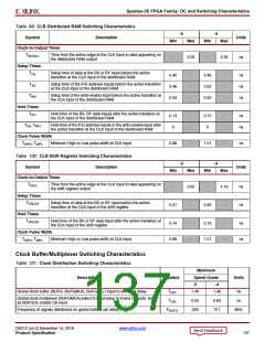
Table 99: CLB Distributed RAM Switching Characteristics
-5
-4
Symbol
Description
Units
Min
Max
Min
Max
Clock-to-Output Times
TSHCKO
Time from the active edge at the CLK input to data appearing on
the distributed RAM output
-
2.05
-
2.35
ns
Setup Times
TDS
Setup time of data at the BX or BY input before the active
transition at the CLK input of the distributed RAM
0.40
0.46
0.34
-
-
-
0.46
0.52
0.40
-
-
-
ns
ns
ns
TAS
Setup time of the F/G address inputs before the active transition
at the CLK input of the distributed RAM
TWS
Setup time of the write enable input before the active transition at
the CLK input of the distributed RAM
Hold Times
TDH
Hold time of the BX, BY data inputs after the active transition at
the CLK input of the distributed RAM
0.13
0
-
-
0.15
0
-
-
ns
ns
T
AH, TWH
Hold time of the F/G address inputs or the write enable input after
the active transition at the CLK input of the distributed RAM
Clock Pulse Width
TWPH, TWPL
Minimum High or Low pulse width at CLK input
0.88
-
1.01
-
ns
Table 100: CLB Shift Register Switching Characteristics
-5
-4
Symbol
Description
Units
Min
Max
Min
Max
Clock-to-Output Times
TREG
Time from the active edge at the CLK input to data appearing on
the shift register output
-
3.62
-
4.16
ns
ns
Setup Times
TSRLDS
Setup time of data at the BX or BY input before the active
transition at the CLK input of the shift register
0.41
-
0.46
-
Hold Times
TSRLDH
Hold time of the BX or BY data input after the active transition at
the CLK input of the shift register
0.14
0.88
-
-
0.16
1.01
-
-
ns
ns
Clock Pulse Width
TWPH, TWPL
Minimum High or Low pulse width at CLK input
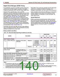
Clock Buffer/Multiplexer Switching Characteristics
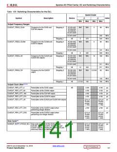
Table 101: Clock Distribution Switching Characteristics
Maximum
Speed Grade
Description
Symbol
Units
-5
-4
Global clock buffer (BUFG, BUFGMUX, BUFGCE) I input to O-output delay
TGIO
TGSI
1.46
1.46
0.63
311
ns
ns
Global clock multiplexer (BUFGMUX) select S-input setup to I0 and I1 inputs. Same
as BUFGCE enable CE-input
0.55
333
Frequency of signals distributed on global buffers (all sides)
FBUFG
MHz
DS312 (v4.2) December 14, 2018
www.xilinx.com
Product Specification
137

 XILINX [ XILINX, INC ]