Spartan-3E FPGA Family: DC and Switching Characteristics
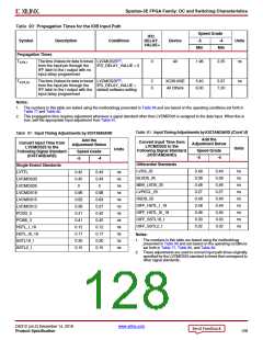
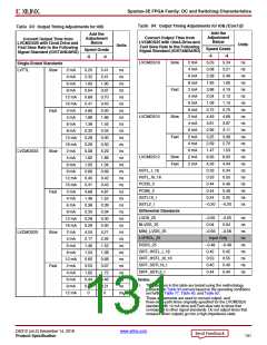
Table 94: Output Timing Adjustments for IOB (Cont’d)
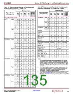
Table 94: Output Timing Adjustments for IOB
Add the
Adjustment
Below
Add the
Adjustment
Below
Convert Output Time from
LVCMOS25 with 12mA Drive and
Fast Slew Rate to the Following
Signal Standard (IOSTANDARD)
Convert Output Time from
LVCMOS25 with 12mA Drive and
Fast Slew Rate to the Following
Signal Standard (IOSTANDARD)
Units
Units
Speed Grade
Speed Grade
-5
-4
-5
-4
LVCMOS18
Slow
2 mA
4 mA
6 mA
8 mA
2 mA
4 mA
6 mA
8 mA
2 mA
4 mA
6 mA
2 mA
4 mA
6 mA
2 mA
2 mA
5.03
3.08
2.39
1.83
3.98
2.04
1.09
0.72
4.49
3.81
2.99
3.25
2.59
1.47
6.36
4.26
0.33
0.53
0.44
0.44
0.24
–0.20
5.24
3.21
2.49
1.90
4.15
2.13
1.14
0.75
4.68
3.97
3.11
3.38
2.70
1.53
6.63
4.44
0.34
0.55
0.46
0.46
0.25
–0.20
ns
ns
ns
ns
ns
ns
ns
ns
ns
ns
ns
ns
ns
ns
ns
ns
ns
ns
ns
ns
ns
ns
Single-Ended Standards
LVTTL
Slow
Fast
Slow
Fast
2 mA
4 mA
6 mA
8 mA
12 mA
16 mA
2 mA
4 mA
6 mA
8 mA
12 mA
16 mA
2 mA
4 mA
6 mA
8 mA
12 mA
16 mA
2 mA
4 mA
6 mA
8 mA
12 mA
16 mA
2 mA
4 mA
6 mA
8 mA
12 mA
2 mA
4 mA
6 mA
8 mA
12 mA
5.20
2.32
1.83
0.64
0.68
0.41
4.80
1.88
1.39
0.32
0.28
0.28
5.08
1.82
1.00
0.66
0.40
0.41
4.68
1.46
0.38
0.33
0.28
0.28
4.04
2.17
1.46
1.04
0.65
3.53
1.65
0.44
0.20
0
5.41
2.41
1.90
0.67
0.70
0.43
5.00
1.96
1.45
0.34
0.30
0.30
5.29
1.89
1.04
0.69
0.42
0.43
4.87
1.52
0.39
0.34
0.30
0.30
4.21
2.26
1.52
1.08
0.68
3.67
1.72
0.46
0.21
0
ns
ns
ns
ns
ns
ns
ns
ns
ns
ns
ns
ns
ns
ns
ns
ns
ns
ns
ns
ns
ns
ns
ns
ns
ns
ns
ns
ns
ns
ns
ns
ns
ns
ns
Fast
LVCMOS15
LVCMOS12
Slow
Fast
LVCMOS33
Slow
Fast
HSTL_I_18
HSTL_III_18
PCI33_3
PCI66_3
SSTL18_I
SSTL2_I
Differential Standards
LVDS_25
–0.55
0.04
–0.55
0.04
ns
ns
ns
ns
ns
ns
ns
ns
ns
BLVDS_25
MINI_LVDS_25
LVPECL_25
–0.56
–0.56
LVCMOS25
Slow
Fast
Input Only
RSDS_25
–0.48
0.42
0.53
0.40
0.44
–0.48
0.42
0.55
0.40
0.44
DIFF_HSTL_I_18
DIFF_HSTL_III_18
DIFF_SSTL18_I
DIFF_SSTL2_I
Notes:
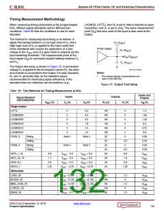
1. The numbers in this table are tested using the methodology
presented in Table 95 and are based on the operating conditions
set forth in Table 77, Table 80, and Table 82.
2. These adjustments are used to convert output- and
three-state-path times originally specified for the LVCMOS25
standard with 12 mA drive and Fast slew rate to times that
correspond to other signal standards. Do not adjust times that
measure when outputs go into a high-impedance state.
DS312 (v4.2) December 14, 2018
www.xilinx.com
Product Specification
131

 XILINX [ XILINX, INC ]