Spartan-3E FPGA Family: DC and Switching Characteristics
Timing Measurement Methodology
When measuring timing parameters at the programmable
I/Os, different signal standards call for different test
conditions. Table 95 lists the conditions to use for each
standard.
LVCMOS, LVTTL), then R is set to 1MΩ to indicate an open
T
connection, and V is set to zero. The same measurement
T
point (V ) that was used at the Input is also used at the
M
Output.
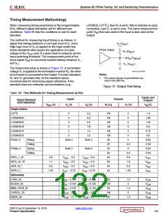
X-Ref Target - Figure 72
The method for measuring Input timing is as follows: A
V (V
)
signal that swings between a Low logic level of V and a
L
T
REF
High logic level of V is applied to the Input under test.
Some standards also require the application of a bias
H
FPGA Output
R (R
T
)
REF
voltage to the V
pins of a given bank to properly set the
REF
input-switching threshold. The measurement point of the
V
(V
)
M
MEAS
Input signal (V ) is commonly located halfway between V
M
L
and V .
C (C
)
H
L
REF
The Output test setup is shown in Figure 72. A termination
voltage V is applied to the termination resistor R , the other
ds312-3_04_090105
T
T
Notes:
end of which is connected to the Output. For each standard,
R and V generally take on the standard values
1. The names shown in parentheses are
used in the IBIS file.
T
T
recommended for minimizing signal reflections. If the
standard does not ordinarily use terminations (e.g.,
Figure 72: Output Test Setup
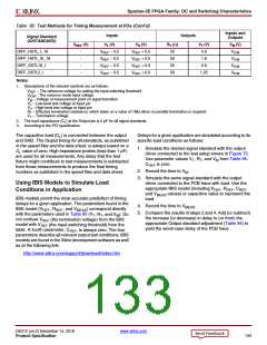
Table 95: Test Methods for Timing Measurement at I/Os
Inputs and
Inputs
Outputs
Signal Standard
(IOSTANDARD)
Outputs
VREF (V)
VL (V)
VH (V)
RT (Ω)
VT (V)
VM (V)
Single-Ended
LVTTL
-
-
-
-
-
-
-
0
3.3
3.3
1M
1M
1M
1M
1M
1M
25
0
0
1.4
1.65
1.25
0.9
LVCMOS33
LVCMOS25
LVCMOS18
LVCMOS15
LVCMOS12
PCI33_3
0
0
2.5
0
0
1.8
0
0
0
1.5
0
0.75
0.6
1.2
0
Rising
Falling
Rising
Falling
Note 3
Note 3
0
0.94
2.03
0.94
2.03
VREF
VREF
VREF
VREF
25
3.3
0
PCI66_3
-
Note 3
Note 3
25
25
3.3
0.9
1.8
0.9
1.25
HSTL_I_18
HSTL_III_18
SSTL18_I
SSTL2_I
0.9
1.1
V
REF – 0.5
VREF + 0.5
VREF + 0.5
VREF + 0.5
VREF + 0.75
50
VREF – 0.5
VREF – 0.5
VREF – 0.75
50
0.9
50
1.25
50
Differential
LVDS_25
-
-
-
-
-
VICM – 0.125
VICM – 0.125
VICM – 0.125
VICM – 0.3
VICM + 0.125
VICM + 0.125
VICM + 0.125
VICM + 0.3
50
1M
50
1.2
0
VICM
VICM
VICM
VICM
VICM
BLVDS_25
MINI_LVDS_25
LVPECL_25
RSDS_25
1.2
0
1M
50
VICM – 0.1
VICM + 0.1
1.2
DS312 (v4.2) December 14, 2018
www.xilinx.com
Product Specification
132

 XILINX [ XILINX, INC ]