Spartan-3E FPGA Family: DC and Switching Characteristics
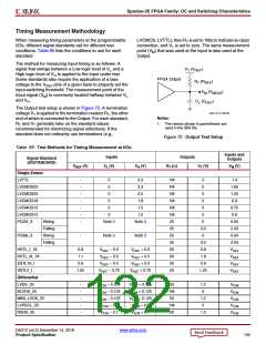
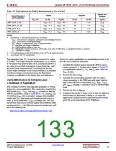
Table 95: Test Methods for Timing Measurement at I/Os (Cont’d)
Inputs and
Outputs
Inputs
Outputs
Signal Standard
(IOSTANDARD)
VREF (V)
VL (V)
VH (V)
RT (Ω)
50
VT (V)
0.9
VM (V)
VICM
VICM
VICM
VICM
DIFF_HSTL_I_18
-
-
-
-
VREF – 0.5
VREF – 0.5
VREF – 0.5
VREF – 0.5
VREF + 0.5
VREF + 0.5
VREF + 0.5
VREF + 0.5
DIFF_HSTL_III_18
DIFF_SSTL18_I
DIFF_SSTL2_I
50
1.8
50
0.9
50
1.25
Notes:
1. Descriptions of the relevant symbols are as follows:
V
V
V
– The reference voltage for setting the input switching threshold
– The common mode input voltage
– Voltage of measurement point on signal transition
REF
ICM
M
V – Low-level test voltage at Input pin
L
V
– High-level test voltage at Input pin
H
R – Effective termination resistance, which takes on a value of 1MΩ when no parallel termination is required
T
V – Termination voltage
T
2. The load capacitance (C ) at the Output pin is 0 pF for all signal standards.
L
3. According to the PCI specification.
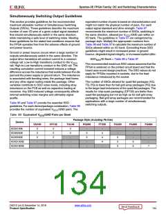
The capacitive load (C ) is connected between the output
and GND. The Output timing for all standards, as published
Delays for a given application are simulated according to its
specific load conditions as follows:
L
in the speed files and the data sheet, is always based on a
1. Simulate the desired signal standard with the output
driver connected to the test setup shown in Figure 72.
C value of zero. High-impedance probes (less than 1 pF)
L
are used for all measurements. Any delay that the test
fixture might contribute to test measurements is subtracted
from those measurements to produce the final timing
numbers as published in the speed files and data sheet.
Use parameter values V , R , and V from Table 95.
T
T
M
C
is zero.
REF
2. Record the time to V .
M
3. Simulate the same signal standard with the output
driver connected to the PCB trace with load. Use the
Using IBIS Models to Simulate Load
Conditions in Application
appropriate IBIS model (including V
, R
, C
,
REF
REF
REF
and V
load.
values) or capacitive value to represent the
MEAS
IBIS models permit the most accurate prediction of timing
delays for a given application. The parameters found in the
4. Record the time to V
.
MEAS
IBIS model (V
, R
, and V
) correspond directly
REF
REF
MEAS
5. Compare the results of steps 2 and 4. Add (or subtract)
the increase (or decrease) in delay to (or from) the
appropriate Output standard adjustment (Table 94) to
yield the worst-case delay of the PCB trace.
with the parameters used in Table 95 (V , R , and V ). Do
T
T
M
not confuse V
(the termination voltage) from the IBIS
REF
model with V
(the input-switching threshold) from the
REF
table. A fourth parameter, C
, is always zero. The four
REF
parameters describe all relevant output test conditions. IBIS
models are found in the Xilinx development software as well
as at the following link:
http://www.xilinx.com/support/download/index.htm
DS312 (v4.2) December 14, 2018
www.xilinx.com
Product Specification
133

 XILINX [ XILINX, INC ]