Spartan-3E FPGA Family: DC and Switching Characteristics
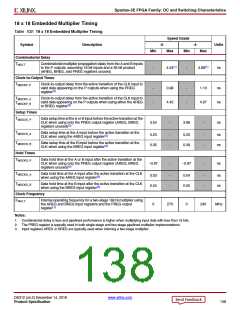
18 x 18 Embedded Multiplier Timing
Table 102: 18 x 18 Embedded Multiplier Timing
Speed Grade
Symbol
Description
-5
-4
Units
Min
Max
Min
Max
Combinatorial Delay
TMULT
Combinatorial multiplier propagation delay from the A and B inputs
to the P outputs, assuming 18-bit inputs and a 36-bit product
(AREG, BREG, and PREG registers unused)
-
4.34(1)
-
4.88(1)
ns
Clock-to-Output Times
TMSCKP_P
Clock-to-output delay from the active transition of the CLK input to
valid data appearing on the P outputs when using the PREG
-
-
0.98
4.42
-
-
1.10
4.97
ns
ns
register(2)
TMSCKP_A
TMSCKP_B
Clock-to-output delay from the active transition of the CLK input to
valid data appearing on the P outputs when using either the AREG
or BREG register(3)
Setup Times
TMSDCK_P
Data setup time at the A or B input before the active transition at the
CLK when using only the PREG output register (AREG, BREG
registers unused)(2)
3.54
-
3.98
-
ns
TMSDCK_A
TMSDCK_B
Data setup time at the A input before the active transition at the
CLK when using the AREG input register(3)
0.20
0.35
-
-
0.23
0.39
-
-
ns
ns
Data setup time at the B input before the active transition at the
CLK when using the BREG input register(3)
Hold Times
TMSCKD_P
Data hold time at the A or B input after the active transition at the
CLK when using only the PREG output register (AREG, BREG
registers unused)(2)
–0.97
-
–0.97
-
ns
TMSCKD_A
TMSCKD_B
Clock Frequency
Data hold time at the A input after the active transition at the CLK
0.03
0.04
-
-
0.04
0.05
-
-
ns
ns
when using the AREG input register(3)
Data hold time at the B input after the active transition at the CLK
when using the BREG input register(3)
FMULT
Internal operating frequency for a two-stage 18x18 multiplier using
the AREG and BREG input registers and the PREG output
0
270
0
240
MHz
register(1)
Notes:
1. Combinatorial delay is less and pipelined performance is higher when multiplying input data with less than 18 bits.
2. The PREG register is typically used in both single-stage and two-stage pipelined multiplier implementations.
3. Input registers AREG or BREG are typically used when inferring a two-stage multiplier.
DS312 (v4.2) December 14, 2018
www.xilinx.com
Product Specification
138

 XILINX [ XILINX, INC ]