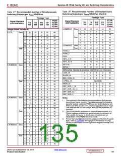
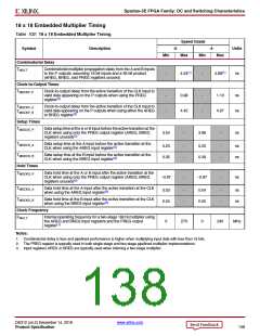
Spartan-3E FPGA Family: DC and Switching Characteristics
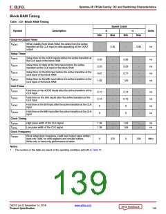
Block RAM Timing
Table 103: Block RAM Timing
Speed Grade
Symbol
Description
-5
-4
Units
Min
Max
Min
Max
Clock-to-Output Times
TBCKO
When reading from block RAM, the delay from the active
transition at the CLK input to data appearing at the DOUT
output
-
2.45
-
2.82
ns
Setup Times
TBACK
Setup time for the ADDR inputs before the active transition at
the CLK input of the block RAM
0.33
0.23
0.67
1.09
-
-
-
-
0.38
0.23
0.77
1.26
-
-
-
-
ns
ns
ns
ns
TBDCK
TBECK
TBWCK
Setup time for data at the DIN inputs before the active
transition at the CLK input of the block RAM
Setup time for the EN input before the active transition at the
CLK input of the block RAM
Setup time for the WE input before the active transition at the
CLK input of the block RAM
Hold Times
TBCKA
Hold time on the ADDR inputs after the active transition at the
CLK input
0.12
0.12
0
-
-
-
-
0.14
0.13
0
-
-
-
-
ns
ns
ns
ns
TBCKD
TBCKE
TBCKW
Hold time on the DIN inputs after the active transition at the
CLK input
Hold time on the EN input after the active transition at the CLK
input
Hold time on the WE input after the active transition at the CLK
input
0
0
Clock Timing
TBPWH
High pulse width of the CLK signal
Low pulse width of the CLK signal
1.39
1.39
-
-
1.59
1.59
-
-
ns
ns
TBPWL
Clock Frequency
FBRAM
Block RAM clock frequency. RAM read output value written
back into RAM, for shift-registers and circular buffers.
Write-only or read-only performance is faster.
0
270
0
230
MHz
Notes:
1. The numbers in this table are based on the operating conditions set forth in Table 77.
DS312 (v4.2) December 14, 2018
www.xilinx.com
Product Specification
139

 XILINX [ XILINX, INC ]