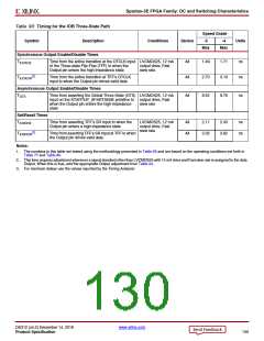
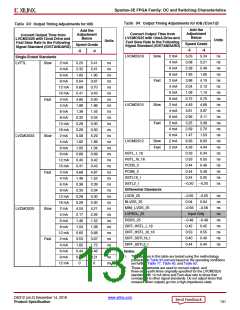
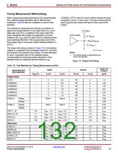
Spartan-3E FPGA Family: DC and Switching Characteristics
Speed Grade
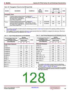
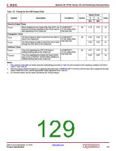
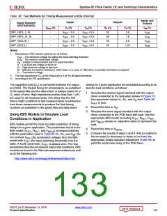
Table 92: Timing for the IOB Output Path
Symbol
Description
Conditions
Device
-5
-4
Units
Min
Min
Clock-to-Output Times
TIOCKP
When reading from the Output Flip-Flop (OFF), the LVCMOS25(2)
time from the active transition at the OCLK input to 12 mA output drive,
data appearing at the Output pin Fast slew rate
,
All
2.18
2.50
ns
Propagation Times
TIOOP
The time it takes for data to travel from the IOB’s O LVCMOS25(2)
,
All
All
2.24
2.32
2.58
2.67
ns
ns
input to the Output pin
12 mA output drive,
Fast slew rate
TIOOLP
The time it takes for data to travel from the O input
through the OFF latch to the Output pin
Set/Reset Times
TIOSRP
Time from asserting the OFF’s SR input to
setting/resetting data at the Output pin
LVCMOS25(2)
12 mA output drive,
Fast slew rate
,
3.27
8.40
3.76
9.65
ns
ns
TIOGSRQ
Time from asserting the Global Set Reset (GSR)
input on the STARTUP_SPARTAN3E primitive to
setting/resetting data at the Output pin
Notes:
1. The numbers in this table are tested using the methodology presented in Table 95 and are based on the operating conditions set forth in
Table 77 and Table 80.
2. This time requires adjustment whenever a signal standard other than LVCMOS25 with 12 mA drive and Fast slew rate is assigned to the data
Output. When this is true, add the appropriate Output adjustment from Table 94.
3. For minimum delays use the values reported by the Timing Analyzer.
DS312 (v4.2) December 14, 2018
www.xilinx.com
Product Specification
129

 XILINX [ XILINX, INC ]