Spartan-3E FPGA Family: DC and Switching Characteristics
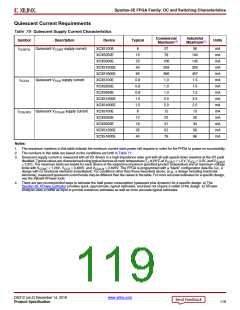
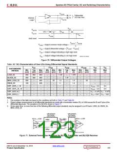
X-Ref Target - Figure 70
VOUTP
Differential
I/O Pair Pins
P
N
Internal
Logic
VOUTN
VOH
VOUTN
VOD
50%
VOUTP
VOL
VOCM
GND level
VOUTP + VOUTN
V
OCM = Output common mode voltage =
2
VOUTP - VOUTN
= Output voltage indicating a High logic level
= Output voltage indicating a Low logic level
V
OD = Output differential voltage =
VOH
VOL
DS312-3_03_021505
Figure 70: Differential Output Voltages
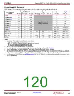
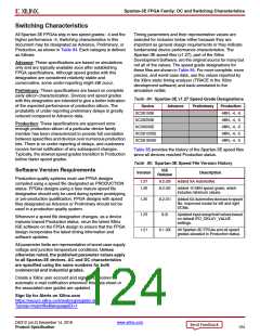
Table 83: DC Characteristics of User I/Os Using Differential Signal Standards
VOD
ΔVOD
Min Max
(mV) (mV)
VOCM
ΔVOCM
VOH
VOL
IOSTANDARD
Attribute
Min
(mV)
Typ
(mV)
Max
(mV)
Min
(V)
Typ
(V)
Max
(V)
Min
Max
Min
(V)
Max
(V)
(mV) (mV)
LVDS_25
250
250
300
100
–
350
350
–
450
450
600
400
–
–
–
–
–
–
–
–
–
–
–
1.125
–
1.20
–
1.375
–
–
–
–
–
–
–
–
–
–
–
–
–
BLVDS_25
–
1.0
1.1
–
–
1.4
1.4
–
–
MINI_LVDS_25
RSDS_25
50
–
50
–
–
–
–
–
–
–
DIFF_HSTL_I_18
DIFF_HSTL_III_18
DIFF_SSTL18_I
DIFF_SSTL2_I
–
–
–
–
VCCO – 0.4
VCCO – 0.4
0.4
0.4
–
–
–
–
–
–
–
–
–
–
–
–
–
–
–
–
VTT + 0.475 VTT – 0.475
VTT + 0.61 VTT – 0.61
–
–
–
–
–
–
–
–
Notes:
1. The numbers in this table are based on the conditions set forth in Table 77 and Table 82.
2. Output voltage measurements for all differential standards are made with a termination resistor (R ) of 100Ω across the N and P pins of the
T
differential signal pair. The exception is for BLVDS, shown in Figure 71.
3. At any given time, no more than two of the following differential output standards may be assigned to an I/O bank: LVDS_25, RSDS_25,
MINI_LVDS_25
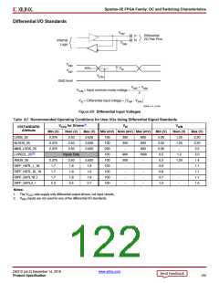
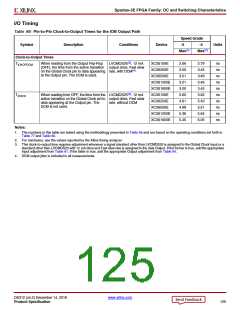
X-Ref Target - Figure 71
1/4th of Bourns
Part Number
CAT16-LV4F12
1/4th of Bourns
Part Number
CAT16-PT4F4
V
CCO = 2.5V
V
CCO = 2.5V
Z
0
0
= 50Ω
= 50Ω
165Ω
FPGA
Out
FPGA
In
140Ω
100Ω
Z
165Ω
ds312-3_07_041108
Figure 71: External Termination Resistors for BLVDS Transmitter and BLVDS Receiver
DS312 (v4.2) December 14, 2018
www.xilinx.com
Product Specification
123

 XILINX [ XILINX, INC ]