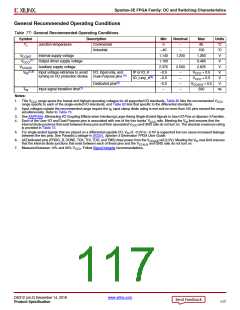
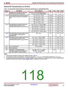
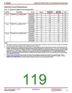
Spartan-3E FPGA Family: DC and Switching Characteristics
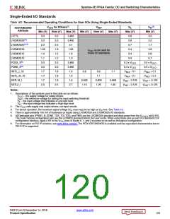
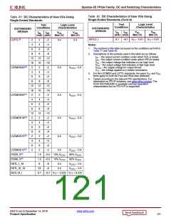
Table 81: DC Characteristics of User I/Os Using
Single-Ended Standards (Cont’d)
Table 81: DC Characteristics of User I/Os Using
Single-Ended Standards
Test
Logic Level
Test
Logic Level
Conditions
Characteristics
Conditions
Characteristics
IOSTANDARD
Attribute
IOSTANDARD
Attribute
IOL
IOH
VOL
VOH
Min (V)
IOL
IOH
VOL
VOH
Min (V)
(mA) (mA)
Max (V)
(mA) (mA)
Max (V)
LVTTL(3)
2
4
6
8
2
4
–2
–4
0.4
2.4
SSTL2_I
Notes:
8.1
–8.1 VTT – 0.61
VTT + 0.61
1. The numbers in this table are based on the conditions set forth in
Table 77 and Table 80.
2. Descriptions of the symbols used in this table are as follows:
6
–6
8
–8
I
I
V
V
V
V
– the output current condition under which VOL is tested
– the output current condition under which VOH is tested
OL
OH
12
16
2
12
16
2
–12
–16
–2
– the output voltage that indicates a Low logic level
– the output voltage that indicates a High logic level
OL
OH
LVCMOS33(3)
0.4
VCCO – 0.4
– the supply voltage for output drivers
CCO
– the voltage applied to a resistor termination
TT
4
4
–4
3. For the LVCMOS and LVTTL standards: the same V and V
OL
OH
limits apply for both the Fast and Slow slew attributes.
6
6
–6
4. Tested according to the relevant PCI specifications. For
information on PCI IP solutions, see www.xilinx.com/pci. The
PCIX IOSTANDARD is available and has equivalent
characteristics but no PCI-X IP is supported.
8
8
–8
12
16
2
12
16
2
–12
–16
–2
LVCMOS25(3)
0.4
0.4
VCCO – 0.4
4
4
–4
6
6
–6
8
8
–8
12
2
12
2
–12
–2
LVCMOS18(3)
LVCMOS15(3)
VCCO – 0.4
4
4
–4
6
6
–6
8
8
–8
2
2
–2
0.4
0.4
VCCO – 0.4
4
4
–4
6
6
–6
LVCMOS12(3)
PCI33_3(4)
PCI66_3(4)
HSTL_I_18
HSTL_III_18
SSTL18_I
2
2
–2
VCCO – 0.4
90% VCCO
90% VCCO
VCCO – 0.4
1.5
1.5
8
–0.5 10% VCCO
–0.5 10% VCCO
–8
–8
0.4
0.4
24
6.7
VCCO – 0.4
–6.7
VTT – 0.475 VTT + 0.475
DS312 (v4.2) December 14, 2018
www.xilinx.com
Product Specification
121

 XILINX [ XILINX, INC ]