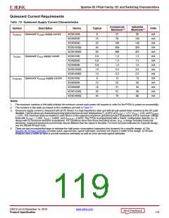
Spartan-3E FPGA Family: DC and Switching Characteristics
Single-Ended I/O Standards
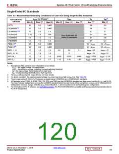
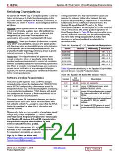
Table 80: Recommended Operating Conditions for User I/Os Using Single-Ended Standards
(3)
V
CCO for Drivers(2)
VREF
VIL
Max (V)
0.8
VIH
IOSTANDARD
Attribute
Min (V)
3.0
Nom (V)
3.3
Max (V)
Min (V)
Nom (V)
Max (V)
Min (V)
2.0
LVTTL
LVCMOS33
3.465
3.465
2.7
(4)
3.0
3.3
0.8
2.0
LVCMOS25(4,5)
LVCMOS18
LVCMOS15
LVCMOS12
2.3
2.5
0.7
1.7
1.65
1.4
1.8
1.95
1.6
0.4
0.8
VREF is not used for
these I/O standards
1.5
0.4
0.8
1.1
1.2
1.3
0.4
0.7
(6)
PCI33_3
3.0
3.3
3.465
3.465
1.9
0.3 • VCCO
0.3 • VCCO
VREF - 0.1
0.5 • VCCO
0.5 • VCCO
VREF + 0.1
VREF + 0.1
VREF + 0.125
VREF + 0.125
(6)
PCI66_3
3.0
3.3
HSTL_I_18
HSTL_III_18
SSTL18_I
SSTL2_I
1.7
1.8
0.8
-
0.9
1.1
1.1
-
1.7
1.8
1.9
V
REF - 0.1
VREF - 0.125
VREF - 0.125
1.7
1.8
1.9
0.833
1.15
0.900
1.25
0.969
1.35
2.3
2.5
2.7
Notes:
1. Descriptions of the symbols used in this table are as follows:
V
V
V
V
– the supply voltage for output drivers
CCO
REF
IL
– the reference voltage for setting the input switching threshold
– the input voltage that indicates a Low logic level
– the input voltage that indicates a High logic level
IH
2. The V
rails supply only output drivers, not input circuits.
CCO
3. For device operation, the maximum signal voltage (V max) may be as high as V max. See Table 73.
IH
IN
4. There is approximately 100 mV of hysteresis on inputs using LVCMOS33 and LVCMOS25 I/O standards.
5. All Dedicated pins (PROG_B, DONE, TCK, TDI, TDO, and TMS) use the LVCMOS25 standard and draw power from the V
rail (2.5V).
CCAUX
The Dual-Purpose configuration pins use the LVCMOS standard before the User mode. When using these pins as part of a standard 2.5V
configuration interface, apply 2.5V to the V lines of Banks 0, 1, and 2 at power-on as well as throughout configuration.
CCO
6. For information on PCI IP solutions, see www.xilinx.com/pci. The PCIX IOSTANDARD is available and has equivalent characteristics but no
PCI-X IP is supported.
DS312 (v4.2) December 14, 2018
www.xilinx.com
Product Specification
120

 XILINX [ XILINX, INC ]