Spartan-3E FPGA Family: DC and Switching Characteristics
Differential I/O Standards
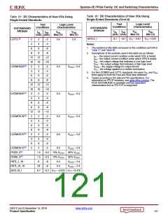
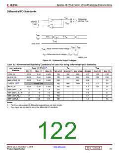
X-Ref Target - Figure 69
VINP
Differential
I/O Pair Pins
P
N
Internal
Logic
VINN
VINN
VID
50%
VINP
VICM
GND level
VINP + VINN
V
ICM = Input common mode voltage =
2
V
VINP - VINN
ID = Differential input voltage =
DS099-3_01_012304
Figure 69: Differential Input Voltages
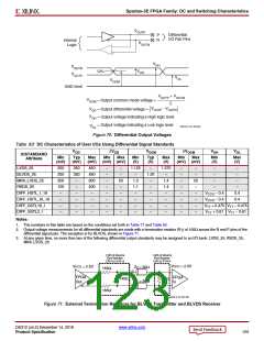
Table 82: Recommended Operating Conditions for User I/Os Using Differential Signal Standards
VCCO for Drivers(1)
VID
VICM
IOSTANDARD
Attribute
Min (V)
2.375
2.375
2.375
Nom (V)
2.50
Max (V)
Min (mV) Nom (mV) Max (mV)
Min (V)
0.30
0.30
0.30
0.5
Nom (V)
Max (V)
2.20
2.20
2.2
LVDS_25
2.625
2.625
2.625
100
100
200
100
100
100
100
100
100
350
600
1.25
BLVDS_25
2.50
350
600
1.25
MINI_LVDS_25
LVPECL_25(2)
RSDS_25
2.50
-
600
-
Inputs Only
2.50
800
1000
1.2
2.0
2.375
1.7
2.625
1.9
200
-
-
-
-
-
0.3
1.20
1.4
DIFF_HSTL_I_18
DIFF_HSTL_III_18
DIFF_SSTL18_I
DIFF_SSTL2_I
1.8
-
-
-
-
0.8
-
-
-
-
1.1
1.7
1.8
1.9
0.8
1.1
1.7
1.8
1.9
0.7
1.1
2.3
2.5
2.7
1.0
1.5
Notes:
1. The V
rails supply only differential output drivers, not input circuits.
CCO
2.
V
inputs are not used for any of the differential I/O standards.
REF
DS312 (v4.2) December 14, 2018
www.xilinx.com
Product Specification
122

 XILINX [ XILINX, INC ]