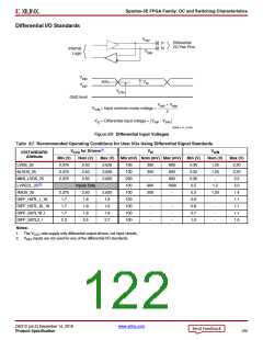
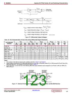
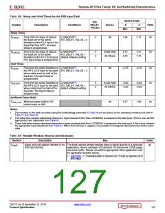
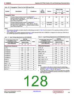
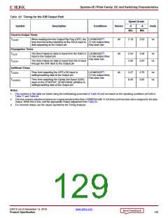
Spartan-3E FPGA Family: DC and Switching Characteristics
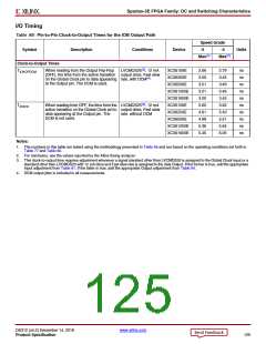
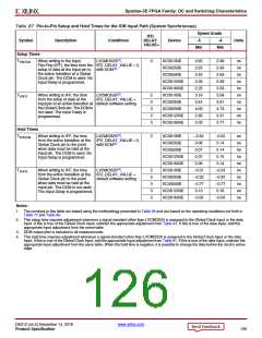
Table 87: Pin-to-Pin Setup and Hold Times for the IOB Input Path (System Synchronous)
Speed Grade
IFD_
DELAY_
VALUE=
Symbol
Description
Conditions
Device
-5
-4
Units
Min
Min
Setup Times
TPSDCM
When writing to the Input
LVCMOS25(2)
,
0
XC3S100E
XC3S250E
XC3S500E
XC3S1200E
XC3S1600E
XC3S100E
XC3S250E
XC3S500E
XC3S1200E
XC3S1600E
2.65
2.25
2.25
2.25
2.25
3.16
3.44
4.00
2.60
3.33
2.98
2.59
2.59
2.58
2.59
3.58
3.91
4.73
3.31
3.77
ns
ns
ns
ns
ns
ns
ns
ns
ns
ns
Flip-Flop (IFF), the time from the IFD_DELAY_VALUE = 0,
setup of data at the Input pin to with DCM(3)
the active transition at a Global
Clock pin. The DCM is used. No
Input Delay is programmed.
TPSFD
When writing to IFF, the time
from the setup of data at the
Input pin to an active transition at default software setting
the Global Clock pin. The DCM is
not used. The Input Delay is
LVCMOS25(2)
IFD_DELAY_VALUE =
,
2
3
3
3
3
programmed.
Hold Times
TPHDCM
When writing to IFF, the time
from the active transition at the
Global Clock pin to the point
when data must be held at the
Input pin. The DCM is used. No
Input Delay is programmed.
LVCMOS25(4)
,
0
XC3S100E
XC3S250E
XC3S500E
XC3S1200E
XC3S1600E
XC3S100E
XC3S250E
XC3S500E
XC3S1200E
XC3S1600E
–0.54
0.06
–0.52
0.14
ns
ns
ns
ns
ns
ns
ns
ns
ns
ns
IFD_DELAY_VALUE = 0,
with DCM(3)
0.07
0.14
0.07
0.15
0.06
0.14
TPHFD
When writing to IFF, the time
from the active transition at the
Global Clock pin to the point
when data must be held at the
Input pin. The DCM is not used.
The Input Delay is programmed.
LVCMOS25(4)
IFD_DELAY_VALUE =
default software setting
,
2
3
3
3
3
–0.31
–0.32
–0.77
0.13
–0.24
–0.32
–0.77
0.16
–0.05
–0.03
Notes:
1. The numbers in this table are tested using the methodology presented in Table 95 and are based on the operating conditions set forth in
Table 77 and Table 80.
2. This setup time requires adjustment whenever a signal standard other than LVCMOS25 is assigned to the Global Clock Input or the data
Input. If this is true of the Global Clock Input, subtract the appropriate adjustment from Table 91. If this is true of the data Input, add the
appropriate Input adjustment from the same table.
3. DCM output jitter is included in all measurements.
4. This hold time requires adjustment whenever a signal standard other than LVCMOS25 is assigned to the Global Clock Input or the data
Input. If this is true of the Global Clock Input, add the appropriate Input adjustment from Table 91. If this is true of the data Input, subtract the
appropriate Input adjustment from the same table. When the hold time is negative, it is possible to change the data before the clock’s active
edge.
DS312 (v4.2) December 14, 2018
www.xilinx.com
Product Specification
126

 XILINX [ XILINX, INC ]