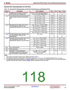
Spartan-3E FPGA Family: DC and Switching Characteristics
General DC Characteristics for I/O Pins
Table 78: General DC Characteristics of User I/O, Dual-Purpose, and Dedicated Pins
Symbol
Description
Test Conditions
Min
Typ
Max
Units
(3)
IL
Leakage current at User I/O, Input-only,
Dual-Purpose, and Dedicated pins
Driver is in a high-impedance state, VIN
0V or VCCO max, sample-tested
=
–10
–
+10
μA
(2)
IRPU
Current through pull-up resistor at User I/O,
Dual-Purpose, Input-only, and Dedicated
pins
V
IN = 0V, VCCO = 3.3V
–0.36
–0.22
–0.10
–0.06
–0.04
2.4
–
–
–
–
–
–
–
–
–
–
–
–1.24
–0.80
–0.42
–0.27
–0.22
10.8
mA
mA
mA
mA
mA
kΩ
kΩ
kΩ
kΩ
VIN = 0V, VCCO = 2.5V
VIN = 0V, VCCO = 1.8V
VIN = 0V, VCCO = 1.5V
VIN = 0V, VCCO = 1.2V
(2)
RPU
Equivalent pull-up resistor value at User
I/O, Dual-Purpose, Input-only, and
Dedicated pins (based on IRPU per Note 2)
VIN = 0V, VCCO = 3.0V to 3.465V
VIN = 0V, VCCO = 2.3V to 2.7V
2.7
11.8
V
IN = 0V, VCCO = 1.7V to 1.9V
4.3
20.2
VIN = 0V, VCCO =1.4V to 1.6V
5.0
25.9
VIN = 0V, VCCO = 1.14V to 1.26V
5.5
32.0
kΩ
mA
(2)
IRPD
Current through pull-down resistor at User
I/O, Dual-Purpose, Input-only, and
Dedicated pins
VIN = VCCO
0.10
0.75
(2)
RPD
Equivalent pull-down resistor value at User
I/O, Dual-Purpose, Input-only, and
Dedicated pins (based on IRPD per Note 2)
V
IN = VCCO = 3.0V to 3.465V
IN = VCCO = 2.3V to 2.7V
VIN = VCCO = 1.7V to 1.9V
IN = VCCO = 1.4V to 1.6V
4.0
3.0
2.3
1.8
1.5
–10
–
–
–
34.5
27.0
19.0
16.0
12.6
+10
10
kΩ
kΩ
kΩ
kΩ
kΩ
μA
pF
Ω
V
–
V
–
VIN = VCCO = 1.14V to 1.26V
–
IREF
CIN
VREF current per pin
Input capacitance
All VCCO levels
–
–
–
RDT
Resistance of optional differential
termination circuit within a differential I/O
pair. Not available on Input-only pairs.
VOCM Min ≤ VICM ≤ VOCM Max
–
120
–
V
OD Min ≤ VID ≤ VOD Max
VCCO = 2.5V
Notes:
1. The numbers in this table are based on the conditions set forth in Table 77.
2. This parameter is based on characterization. The pull-up resistance R = V
/ I
. The pull-down resistance R = V / I
.
PU
CCO RPU
PD
IN RPD
3. For single-ended signals that are placed on a differential-capable I/O, V of –0.2V to –0.5V is supported but can cause increased leakage
IN
between the two pins. See Parasitic Leakage in UG331, Spartan-3 Generation FPGA User Guide.
DS312 (v4.2) December 14, 2018
www.xilinx.com
Product Specification
118

 XILINX [ XILINX, INC ]