Spartan-3E FPGA Family: DC and Switching Characteristics
General Recommended Operating Conditions
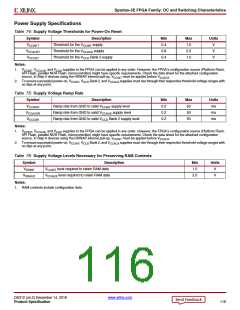
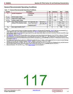
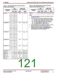
Table 77: General Recommended Operating Conditions
Symbol
Description
Commercial
Min
0
Nominal
Max
85
Units
°C
°C
V
TJ
Junction temperature
–
Industrial
–40
1.140
1.100
2.375
–0.5
–0.5
–0.5
–
–
100
VCCINT
Internal supply voltage
Output driver supply voltage
Auxiliary supply voltage
1.200
1.260
(1)
VCCO
-
3.465
V
VCCAUX
2.500
2.625
V
(2,3)
VIN
Input voltage extremes to avoid
turning on I/O protection diodes
I/O, Input-only, and
IP or IO_#
IO_Lxxy_#(5)
–
–
–
–
VCCO + 0.5
VCCO + 0.5
VCCAUX + 0.5
500
V
Dual-Purpose pins (4)
V
Dedicated pins(6)
V
TIN
Notes:
1. This V
Input signal transition time(7)
ns
range spans the lowest and highest operating voltages for all supported I/O standards. Table 80 lists the recommended V
CCO
CCO
range specific to each of the single-ended I/O standards, and Table 82 lists that specific to the differential standards.
2. Input voltages outside the recommended range require the I input clamp diode rating is met and no more than 100 pins exceed the range
IK
simultaneously. Refer to Table 73.
3. See XAPP459: Eliminating I/O Coupling Effects when Interfacing Large-Swing Single-Ended Signals to User I/O Pins on Spartan-3 Families.
4. Each of the User I/O and Dual-Purpose pins is associated with one of the four banks’ V
rails. Meeting the V limit ensures that the
CCO
IN
internal diode junctions that exist between these pins and their associated V
is provided in Table 73.
and GND rails do not turn on. The absolute maximum rating
CCO
5. For single-ended signals that are placed on a differential-capable I/O, V of –0.2V to –0.5V is supported but can cause increased leakage
IN
between the two pins. See Parasitic Leakage in UG331, Spartan-3 Generation FPGA User Guide.
6. All Dedicated pins (PROG_B, DONE, TCK, TDI, TDO, and TMS) draw power from the V
rail (2.5V). Meeting the V max limit ensures
CCAUX
IN
that the internal diode junctions that exist between each of these pins and the V
and GND rails do not turn on.
CCAUX
7. Measured between 10% and 90% V
. Follow Signal Integrity recommendations.
CCO
DS312 (v4.2) December 14, 2018
www.xilinx.com
Product Specification
117

 XILINX [ XILINX, INC ]