Spartan-3E FPGA Family: DC and Switching Characteristics
Power Supply Specifications
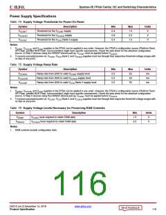
Table 74: Supply Voltage Thresholds for Power-On Reset
Symbol
VCCINTT
VCCAUXT
VCCO2T
Description
Threshold for the VCCINT supply
Min
0.4
0.8
0.4
Max
1.0
Units
V
V
V
Threshold for the VCCAUX supply
2.0
Threshold for the VCCO Bank 2 supply
1.0
Notes:
1.
V
, V
, and V
supplies to the FPGA can be applied in any order. However, the FPGA’s configuration source (Platform Flash,
CCINT
CCAUX
CCO
SPI Flash, parallel NOR Flash, microcontroller) might have specific requirements. Check the data sheet for the attached configuration
source. In Step 0 devices using the HSWAP internal pull-up, V must be applied before V
.
CCAUX
CCINT
2. To ensure successful power-on, V
no dips at any point.
, V
Bank 2, and V
supplies must rise through their respective threshold-voltage ranges with
CCINT CCO
CCAUX
Table 75: Supply Voltage Ramp Rate
Symbol
Description
Min
0.2
0.2
0.2
Max
50
Units
ms
VCCINTR
VCCAUXR
VCCO2R
Ramp rate from GND to valid VCCINT supply level
Ramp rate from GND to valid VCCAUX supply level
Ramp rate from GND to valid VCCO Bank 2 supply level
50
ms
50
ms
Notes:
1.
V
, V
, and V
supplies to the FPGA can be applied in any order. However, the FPGA’s configuration source (Platform Flash,
CCINT
CCAUX
CCO
SPI Flash, parallel NOR Flash, microcontroller) might have specific requirements. Check the data sheet for the attached configuration
source. In Step 0 devices using the HSWAP internal pull-up, V must be applied before V
.
CCAUX
CCINT
2. To ensure successful power-on, V
no dips at any point.
, V
Bank 2, and V
supplies must rise through their respective threshold-voltage ranges with
CCINT CCO
CCAUX
Table 76: Supply Voltage Levels Necessary for Preserving RAM Contents
Symbol
VDRINT
Description
VCCINT level required to retain RAM data
VCCAUX level required to retain RAM data
Min
1.0
2.0
Units
V
V
VDRAUX
Notes:
1. RAM contents include configuration data.
DS312 (v4.2) December 14, 2018
www.xilinx.com
Product Specification
116

 XILINX [ XILINX, INC ]