Philips Semiconductors
Preliminary specification
320 macrocell SRAM CPLD
PZ3320C/PZ3320N
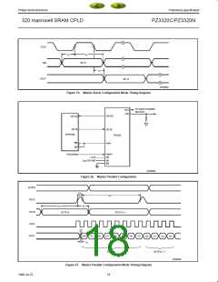
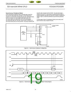
all of the data is loaded into the PZ3320. The serial data begins
shifting out on dout 0.5 cycles after the parallel data was loaded. It
requires additional cclks after the last byte is loaded to complete the
shifting. Figure 22 shows the interface for synchronous peripheral
mode.
Synchronous Peripheral Mode
In the synchronous peripheral mode, byte-wide data is input into
D[7:0] on the rising edge of the cclk input. The first data byte is
clocked in on the second cclk after initn goes high. Subsequent data
bytes are clocked in on every eighth rising edge of cclk. The
rdy_busyn signal is an output which acts as an acknowledge.
rdy_busyn goes high one cclk after a byte of data is clocked in on
D[7:0] and returns low one cclk cycle later. The process repeats until
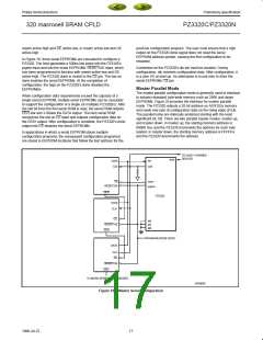
As with master modes, the peripheral modes can be used as the
lead PZ3320 for daisy-chained PZ3320s.
TO DAISY-CHAINED
DEVICES
8
D[7:0]
dout
done
initn
cclk
MICRO–
PROCESSOR
OR
prgmn
SYSTEM
+3.3V
PZ3320
cs1
cs0n
M2
M1
M0
SP00660
Figure 22. Synchronous Peripheral Configuration
t
CH
CCLK
CS0N
t
CL
CS1
INIT
t
H
t
S
D[7:0]
DOUT
BYTE 0
BYTE 1
D7
t
D
D0
D1
D2
D3
D4
D5
D6
D0
D1
RDY/BUSY
SP00609
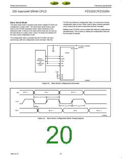
Figure 23. Synchronous Peripheral Configuration Mode Timing Diagram
19
1998 Jul 22

 XILINX [ XILINX, INC ]