Philips Semiconductors
Preliminary specification
320 macrocell SRAM CPLD
PZ3320C/PZ3320N
The Philips PZ3320’s JTAG interface includes a TAP Port and a TAP
Controller, both of which are defined by the IEEE 1149.1 JTAG
Specification. As implemented in the Philips PZ3320, the TAP Port
includes five pins (refer to Table 5) described in the JTAG
specification: tck, tms, tdi, tdo, and trstn. These pins should be
connected to an external pull-up resistor to keep the JTAG signals
from floating when they are not being used.
JTAG Testing Capability
JTAG is the commonly-used acronym for the Boundary Scan Test
(BST) feature defined for integrated circuits by IEEE Standard
1149.1. This standard defines input/output pins, logic control
functions, and commands which facilitate both board and device
level testing without the use of specialized test equipment. BST
provides the ability to test the external connections of a device, test
the internal logic of the device, and capture data from the device
during normal operation. BST provides a number of benefits in each
of the following areas:
Table 6 defines the dedicated pins used by the mandatory JTAG
signals for the PZ3320.
The JTAG specifications define two sets of commands to support
boundary-scan testing: high-level commands and low-level
commands. High-level commands are executed via board test
software on an a user test station such as automated test
equipment, a PC, or an engineering workstation (EWS). Each
high-level command comprises a sequence of low level commands.
These low-level commands are executed within the component
under test, and therefore must be implemented as part of the TAP
Controller design. The set of low-level boundary-scan commands
implemented in the PZ3320 is defined in Table 7. By supporting this
set of low-level commands, the PZ3320 allows execution of all
high-level boundary-scan commands.
• Testability
– Allows testing of an unlimited number of interconnects on the
printed circuit board
– Testability is designed in at the component level
– Enables desired signal levels to be set at specific pins (Preload)
– Data from pin or core logic signals can be examined during
normal operation
• Reliability
– Eliminates physical contacts common to existing test fixtures
(e.g., “bed-of-nails”)
– Degradation of test equipment is no longer a concern
– Facilitates the handling of smaller, surface-mount components
– Allows for testing when components exist on both sides of the
printed circuit board
• Cost
– Reduces/eliminates the need for expensive test equipment
– Reduces test preparation time
– Reduces spare board inventories
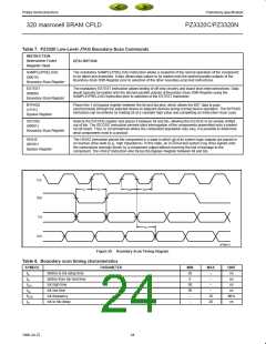
Table 5. JTAG Pin Description
PIN
tck
NAME
DESCRIPTION
Test Clock Output
Clock pin to shift the serial data and instructions in and out of the tdi and tdo pins, respectively. tck is
also used to clock the TAP Controller state machine.
tms
Test Mode Select
Serial input pin selects the JTAG instruction mode. tms should be driven high during user mode
operation.
tdi
Test Data Input
Serial input pin for instructions and test data. Data is shifted in on the rising edge of tck.
tdo
Test Data Output
Serial output pin for instructions and test data. Data is shifted out on the falling edge of tck. The
signal is tri-stated if data is not being shifted out of the device.
trstn
Test Reset
Forces TAP controller to test logic reset state. This signal is active low.
Table 6. PZ3320 JTAG Pinout by Package Type
(PIN NUMBER / MACROCELL #)
tdi
DEVICE
tck
tms
tdo
trstn
23
1998 Jul 22

 XILINX [ XILINX, INC ]