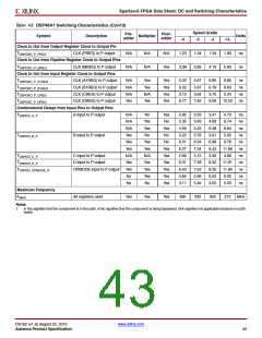
Spartan-6 FPGA Data Sheet: DC and Switching Characteristics
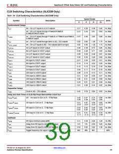
CLB Switching Characteristics (SLICEM Only)
Table 39: CLB Switching Characteristics (SLICEM Only)
Speed Grade
Symbol
Description
Units
-4
-3
-2
-1L
Combinatorial Delays
TILO
An – Dn LUT inputs to A to D outputs
0.21
0.37
0.26
0.43
0.38
0.61
0.49
0.80
ns, Max
ns, Max
An – Dn LUT inputs through F7AMUX/F7BMUX
to AMUX/CMUX output
TOPAB
An – Dn LUT inputs through F7AMUX or F7BMUX and F8MUX
to BMUX output
0.37
0.46
0.65
0.86
ns, Max
TITO
An – Dn LUT inputs through latch to AQ – DQ outputs
An – Dn LUT inputs to AQ – DQ outputs (latch as logic)
An LUT inputs to COUT output
Bn LUT inputs to COUT output
Cn LUT inputs to COUT output
Dn LUT inputs to COUT output
AX input to COUT output
0.82
0.82
0.38
0.38
0.28
0.28
0.21
0.13
0.10
0.09
0.08
0.21
0.30
0.29
0.31
0.95
0.95
0.48
0.49
0.33
0.35
0.26
0.16
0.12
0.11
0.10
0.22
0.31
0.31
0.32
1.28
1.28
0.72
0.71
0.49
0.48
0.40
0.24
0.18
0.14
0.13
0.29
0.46
0.41
0.44
1.70
1.70
0.95
0.92
0.67
0.63
0.51
0.35
0.18
0.18
0.11
0.47
0.58
0.59
0.67
ns, Max
ns, Max
ns, Max
ns, Max
ns, Max
ns, Max
ns, Max
ns, Max
ns, Max
ns, Max
ns, Max
ns, Max
ns, Max
ns, Max
ns, Max
TTITO_LOGIC
TOPCYA
TOPCYB
TOPCYC
TOPCYD
TAXCY
TBXCY
BX input to COUT output
TCXCY
CX input to COUT output
TDXCY
DX input to COUT output
TBYP
CIN input to COUT output
TCINA
CIN input to AMUX output
TCINB
CIN input to BMUX output
TCINC
CIN input to CMUX output
TCIND
CIN input to DMUX output
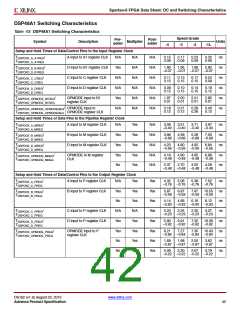
Sequential Delays
TCKO
Clock to AQ – DQ outputs
0.45
0.53
0.64
0.82
ns, Max
Setup and Hold Times of CLB Flip-Flops Before/After Clock CLK
TDICK/TCKDI
AX – DX input to CLK on A – D flip-flops
CE input to CLK on A – D flip-flops
SR input to CLK on A – D flip-flops
CIN input to CLK on A – D flip-flops
0.42
0.28
0.47
0.39
0.74
0.54
0.99
0.58
ns, Min
ns, Min
ns, Min
ns, Min
T
T
T
CECK/TCKCE
SRCK/TCKSR
CINCK/TCKCIN
0.31
–0.07
0.37
–0.07
0.59
–0.07
0.59
–0.27
0.34
0.02
0.42
0.02
0.49
0.02
0.63
–0.33
0.31
–0.17
0.31
–0.13
0.49
–0.12
0.79
–0.46
Set/Reset
TRPW
TRQ
SR input minimum pulse width
0.41
1.81
0.53
862
0.48
1.81
0.65
806
0.65
2.50
0.92
667
1.58
3.05
1.36
ns, Min
ns, Max
ns, Max
MHz
Delay from SR input to AQ – DQ flip-flops
Delay from CE input to AQ – DQ flip-flops
Toggle frequency (for export control)
TCEO
FTOG
DS162 (v1.9) August 23, 2010
www.xilinx.com
Advance Product Specification
39

 XILINX [ XILINX, INC ]