Spartan-6 FPGA Data Sheet: DC and Switching Characteristics
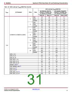
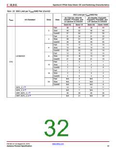
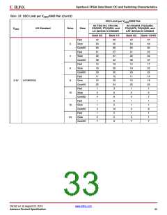
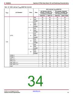
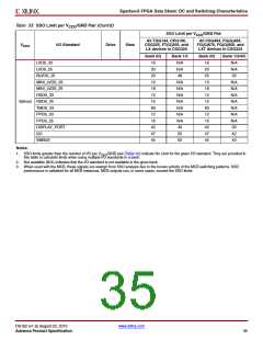
Table 33: SSO Limit per VCCO/GND Pair (Cont’d)
SSO Limit per V
/GND Pair
CCO
All TQG144, CPG196,
CSG225, FT(G)256, and
LX devices in CSG324
All CSG484, FG(G)484,
FG(G)676, FG(G)900, and
LXT devices in CSG324
V
I/O Standard
Drive
Slew
CCO
Bank 0/2
16
Bank 1/3
N/A
N/A
48
Bank 0/2
16
Bank 1/3/4/5
N/A
N/A
20
LVDS_33
LVDS_25
BLVDS_25
20
20
20
20
MINI_LVDS_33
MINI_LVDS_25
RSDS_33
13
N/A
N/A
N/A
N/A
N/A
N/A
N/A
40
13
N/A
N/A
N/A
N/A
N/A
N/A
N/A
30
18
18
12
12
Various RSDS_25
TMDS_33
15
15
83
83
PPDS_33
12
12
PPDS_25
16
16
DISPLAY_PORT
42
42
I2C
47
55
47
42
SMBUS
44
52
44
40
Notes:
1. SSO limits greater than the number of I/O per V
/GND pair (Table 32) indicate No Limit for the given I/O standard. They are provided in
CCO
this table to calculate limits when using multiple I/O standards in a bank.
2. Not available (N/A) indicates that the I/O standard is not available in the given bank.
3. When used with the MCB, these signals are exempt from SSO analysis due to the known activity of the MCB switching patterns. SSO
performance is validated for all MCB instances. MCB outputs can, in some cases, exceed the SSO limits.
DS162 (v1.9) August 23, 2010
www.xilinx.com
Advance Product Specification
35

 XILINX [ XILINX, INC ]