Spartan-6 FPGA Data Sheet: DC and Switching Characteristics
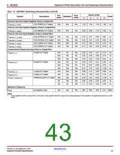
Block RAM Switching Characteristics
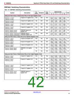
Table 42: Block RAM Switching Characteristics
Speed Grade
Symbol
Description
Units
-4
-3
-2
-1L
Block RAM Clock to Out Delays
TRCKO_DO
Clock CLK to DOUT output (without output register)(1) 1.85
2.10
1.75
2.90
1.90
3.50 ns, Max
2.30 ns, Max
Clock CLK to DOUT output (with output register)(2)
1.60
TRCKO_DO_REG
Setup and Hold Times Before/After Clock CLK
T
T
T
T
T
RCCK_ADDR/TRCKC_ADDR
ADDR inputs(3)
0.35
0.10
0.40
0.12
0.40
0.15
0.50
0.15
ns, Min
ns, Min
ns, Min
ns, Min
ns, Min
RDCK_DI/TRCKD_DI
DIN inputs (4)
0.30
0.10
0.30
0.10
0.30
0.12
0.40
0.15
RCCK_EN/TRCKC_EN
Block RAM Enable (EN) input
CE input of output register
Write Enable (WE) input
0.21
0.05
0.22
0.06
0.28
0.10
0.26
0.10
RCCK_REGCE/TRCKC_REGCE
RCCK_WE/TRCKC_WE
0.20
0.10
0.20
0.10
0.25
0.12
0.28
0.15
0.25
0.10
0.33
0.10
0.46
0.12
0.28
0.15
Maximum Frequency
FMAX
Block RAM in all modes
320
280
260
150
MHz
Notes:
1.
2.
T
T
includes T
and T
as well as the B port equivalent timing parameters.
RCKO_DOPA
RCKO_DO
RCKO_DO_REG
RCKO_DOA
includes T
and T
as well as the B port equivalent timing parameters.
RCKO_DOA_REG
RCKO_DOPA_REG
3. The ADDR setup and hold must be met when EN is asserted (even when WE is deasserted). Otherwise, block RAM data corruption is possible.
4. includes both A and B inputs as well as the parity inputs of A and B.
T
RDCK_DI
DS162 (v1.9) August 23, 2010
www.xilinx.com
Advance Product Specification
41

 XILINX [ XILINX, INC ]