WM8774
Product Preview
In left justified, right justified and I2S modes, the minimum number of BCLKs per DACLRC/ADCLRC
period is 2 times the selected word length. ADCLRC/DACLRC must be high for a minimum of word
length BCLKs and low for a minimum of word length BCLKs. Any mark to space ratio on
ADCLRC/DACLRC is acceptable provided the above requirements are met.
In DSP early or DSP late mode, multiple DACs channel can be time multiplexed onto DIN. DACLRC
is used as a frame sync signal to identify the MSB of the first word. The minimum number of BCLKs
per DACLRC period is 8 times the selected word length. Any mark to space ratio is acceptable on
DACLRC provided the rising edge is correctly positioned. The ADC data may also be output in DSP
early or late modes, with ADCLRC used as a frame sync to identify the MSB of the first word. The
minimum number of BCLKs per ADCLRC period is 2 times the selected word length
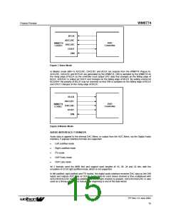
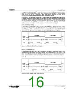
LEFT JUSTIFIED MODE
In left justified mode, the MSB of DIN is sampled by the WM8774 on the first rising edge of BCLK
following a DACLRC transition. The MSB of the ADC data is output on DOUT and changes on the
same falling edge of BCLK as ADCLRC and may be sampled on the rising edge of BCLK. ADCLRC
and DACLRC are high during the left samples and low during the right samples (Figure 9).
1/fs
LEFT CHANNEL
RIGHT CHANNEL
DACLRC/
ADCLRC
BCLK
DIN/
DOUT
1
2
3
n
n-2 n-1
1
2
3
n
n-2 n-1
MSB
LSB
MSB
LSB
Figure 9 Left Justified Mode TIming Diagram
RIGHT JUSTIFIED MODE
In right justified mode, the LSB of DIN is sampled by the WM8774 on the rising edge of BCLK
preceding a DACLRC transition. The LSB of the ADC data is output on DOUT and changes on the
falling edge of BCLK preceding an ADCLRC transition and may be sampled on the rising edge of
BCLK. ADCLRC and DACLRC are high during the left samples and low during the right samples (
Figure 10).
1/fs
LEFT CHANNEL
RIGHT CHANNEL
DACLRC/
ADCLRC
BCLK
DIN/
DOUT
1
2
3
n
1
2
3
n
n-2 n-1
n-2 n-1
MSB
LSB
MSB
LSB
Figure 10 Right Justified Mode Timing Diagram
PP Rev 1.0 June 2002
16
ꢀꢀ

 WOLFSON [ WOLFSON MICROELECTRONICS PLC ]