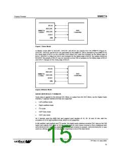
Product Preview
WM8774
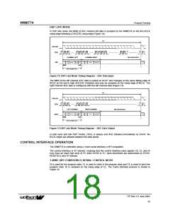
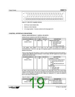
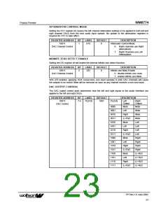
CE
CL
DI
B15
B14
B13
B12
B11
B10
B9
B8
B7
B6
B5
B4
B3
B2
B1
B0
Figure 16 3-Wire SPI Compatible Interface
1. B[15:9] are Control Address Bits
2. B[8:0] are Control Data Bits
3. CE is edge sensitive – the data is latched on the rising edge of CE.
CONTROL INTERFACE REGISTERS
DIGITAL AUDIO INTERFACE CONTROL REGISTER
Interface format is selected via the FMT[1:0] register bits:
REGISTER ADDRESS
10110
BIT
LABEL
DEFAULT
DESCRIPTION
1:0
FMT[1:0]
10
Interface format Select
Interface Control
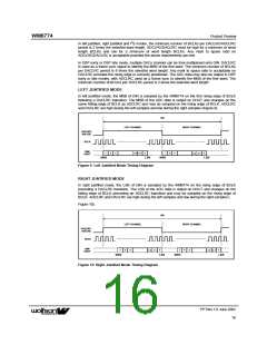
00 : right justified mode
01: left justified mode
10: I2S mode
11: DSP (early or late) mode
In left justified, right justified or I2S modes, the LRP register bit controls the polarity of
ADCLRC/DACLRC. If this bit is set high, the expected polarity of ADCLRC/DACLRC will be the
opposite of that shown,
Figure 10 and. Note that if this feature is used as a means of swapping the left and right channels, a
1 sample phase difference will be introduced. In DSP modes, the LRP register bit is used to select
between early and late modes.
REGISTER ADDRESS
10110
BIT
LABEL
DEFAULT
DESCRIPTION
In left/right/ I2S modes:
2
LRP
0
Interface Control
ADCLRC/DACLRC Polarity (normal)
0 : normal ADCLRC/DACLRC
polarity
1: inverted ADCLRC/DACLRC
polarity
In DSP mode:
0 : Early DSP mode
1: Late DSP mode
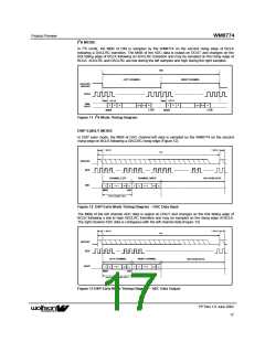
By default, ADCLRC/DACLRC and DIN is sampled on the rising edge of BCLK and should ideally
change on the falling edge. Data sources that change ADCLRC/DACLRC and DIN on the rising edge
of BCLK can be supported by setting the BCP register bit. Setting BCP to 1 inverts the polarity of
BCLK to the inverse of that shown in,
Figure 10, Figure 11, Figure 12, Figure 13, Figure 14 and Figure 15.
REGISTER ADDRESS
10110
BIT
LABEL
DEFAULT
DESCRIPTION
BCLK Polarity (DSP modes)
0 : normal BCLK polarity
1: inverted BCLK polarity
3
BCP
0
Interface Control
PP Rev 1.0 June 2002
19
ꢀꢀ

 WOLFSON [ WOLFSON MICROELECTRONICS PLC ]