WM8774
Product Preview
DEVICE DESCRIPTION
INTRODUCTION
WM8774 is a complete 2-channel DAC, 2-channel ADC audio codec, with flexible input multiplexor
including digital interpolation and decimation filters, multi-bit sigma delta stereo ADC, and switched
capacitor multi-bit sigma delta DACs with analogue volume controls on each channel and output
smoothing filters. It is available in a single package and controlled by a single interface.
An analogue bypass path option is available, to allow stereo analogue signals from any of the 8
stereo inputs to be sent to the stereo outputs via the main volume controls. This allows a purely
analogue input to analogue output high quality signal path to be implemented if required.
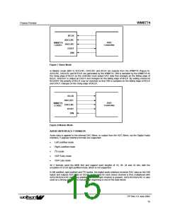
The DAC and ADC have separate left/right clocks and data I/Os. However, BITCLK and MCLK are
shared between the ADC and DAC. The Audio Interface may be configured to operate in either
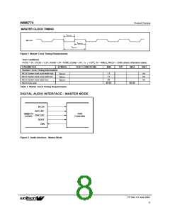
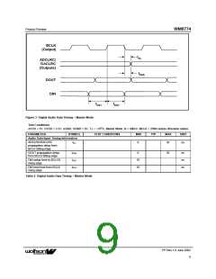
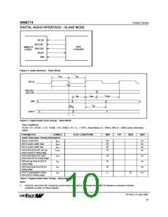
master or slave mode. In Slave mode ADCLRC, DACLRC and BCLK are all inputs. In Master mode
ADCLRC, DACLRC and BCLK are outputs.
The input multiplexor to the ADC is configured to allow large signal levels to be input to the ADC,
using external resistors to reduce the amplitude of larger signals to within the normal operating range
of the ADC. The ADC input PGA also allows input signals to be gained up to +19dB and attenuated
down to -12dB. This allows the user maximum flexibility in the use of the ADC.
A selectable stereo record output is also provided on RECL/R. It is intended that the RECL/R outputs
are only used to drive a high impedance buffer.
The DAC has its own analogue and separate digital volume control. The analogue volume control is
adjustable in 1dB steps and the digital volume control in 0.5dB steps. The analogue and digital
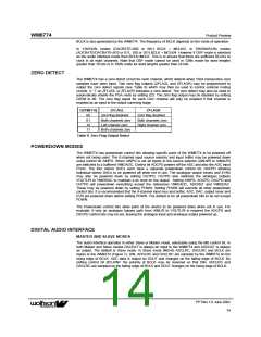
volume controls may be operated independently. In addition a zero cross detect circuit is provided for
both analogue and digital volume controls. When analogue volume zero-cross detection is enabled
the attenuation values are only updated when the input signal to the gain stage is close to the
analogue ground level. The digital volume control detects a transition through the zero point before
updating the volume. This minimises audible clicks and ‘zipper’ noise as the gain values change.
The DAC output incorporates an input selector and mixer allowing an signal to be either switched into
the signal path in place of the DAC signal or mixed with the DAC signal before the volume control.
Use of external resistors allows larger input levels to be accepted by the device, giving maximum
user flexibility.
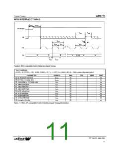
Control of internal functionality of the device is by 3-wire serial control interface. An SPI type control
interface is used, which may be asynchronous to the audio data interface as control data will be re-
synchronised to the audio processing internally.
CE, CL, DI and RESETB are 5V tolerant with TTL input thresholds, allowing the WM8774 to used
with DVDD = 3.3V and be controlled by a controller with 5V output.
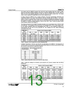
Operation using system clock of 128fs, 192fs, 256fs, 384fs, 512fs or 768fs is provided. In Slave
mode selection between clock rates is automatically controlled. In master mode the master clock to
sample rate ratio is set by control bits ADCRATE and DACRATE. ADC and DAC may run at different
rates within the constraint of a common master clock for the ADC and DACs. For example with
master clock at 24.576MHz, a DAC sample rate of 96kHz (256fs mode) and an ADC sample rate of
48kHz (512fs mode) can be accommodated. Master clock sample rates (fs) from less than 8kHz up
to 192kHz are allowed, provided the appropriate system clock is input.
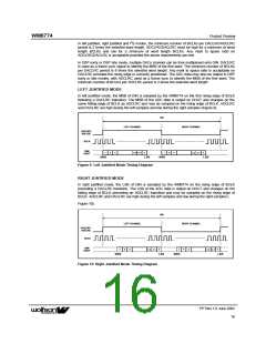
The audio data interface supports right, left and I2S interface formats along with a highly flexible DSP
serial port interface.
AUDIO DATA SAMPLING RATES
In a typical digital audio system there is only one central clock source producing a reference clock to
which all audio data processing is synchronised. This clock is often referred to as the audio system’s
Master Clock. The external master system clock can be applied directly through the MCLK input pin
with no software configuration necessary. In a system where there are a number of possible sources
for the reference clock it is recommended that the clock source with the lowest jitter be used to
optimise the performance of the ADC and DAC.
PP Rev 1.0 June 2002
ꢀꢀ
12

 WOLFSON [ WOLFSON MICROELECTRONICS PLC ]