WM8774
Product Preview
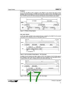
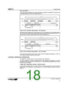
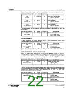
DSP LATE MODE
In DSP late mode, the MSB of DAC channel left data is sampled by the WM8774 on the first BCLK
rising edge following a DACLRC rising edge (Figure 14).
1/fs
DACLRC
BCK
CHANNEL LEFT
CHANNEL RIGHT
NO VALID DATA
DIN
1
2
n
1
2
n
1
n-1
n-1
MSB
LSB
Word Length (WL)
Figure 14 DSP Late Mode Timing Diagram – DAC Data Input
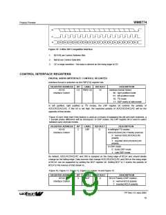
The MSB of the left channel ADC data is output on DOUT and changes on the same falling edge of
BCLK as the low to high ADCLRC transition and may be sampled on the rising edge of BCLK. The
right channel ADC data is contiguous with the left channel data (Figure 15).
1/fs
ADCLRC
BCK
LEFT CHANNEL
RIGHT CHANNEL
NO VALID DATA
1
2
n
1
2
n
1
DOUT
n-1
n-1
MSB
LSB
Word Length (WL)
Figure 15 DSP Late Mode Timing Diagram – ADC Data Output
In both early and late DSP modes, DACL is always sent first, followed immediately by DACR. No
BCLK edges are allowed between the data words.
CONTROL INTERFACE OPERATION
The WM8774 is controlled using a 3-wire serial interface a SPI compatible.
The control interface is 5V tolerant, meaning that the control interface input signals CE, CL and DI
may have an input high level of 5V while DVDD is 3V. Input thresholds are determined by DVDD.
RESETB is also 5V tolerant.
3-WIRE (SPI COMPATIBLE) SERIAL CONTROL MODE
DI is used for the program data, CL is used to clock in the program data and CE is used to latch the
program data. DI is sampled on the rising edge of CL. The 3-wire interface protocol is shown in
Figure 16.
PP Rev 1.0 June 2002
ꢀꢀ
18

 WOLFSON [ WOLFSON MICROELECTRONICS PLC ]