Production Data
WM8352
Note: If a GPIO pin is configured as an open drain output, (ie. GPn_DIR=0, GPn_CFG=1), then the
external pull-up voltage must not be greater than the supply domain for the corresponding GPIO. For
example, if the GPIO supply domain is DBVDD then the external pull-up voltage must be less than or
equal to DBVDD.
Note: Do not enable pull-up and pull-down resistors for the same GPIO pin.
Note: The internal pull-up and pull-down on GPIO10, GPIO11 and GPIO12 may be too weak for
many applications. If pull-up or pull-down is required on these pins, it is recommended to ensure that
the pull resistance is <100kΩ. This can be achieved using an external resistor on its own or in
combination with the internal resistance.
20.1.2 INPUT DE-BOUNCE
GPIO inputs have an optional de-bounce function to remove glitches from the input signal. This may
be useful when the GPIO is connected to a mechanical switch. The de-bounce function can be
enabled for each pin individually using GPn_DB, with a globally selectable de-bounce time set by
GP_DBTIME.
GPIO alternative functions PWR_ON, PWR_OFF and /WAKEUP are special cases with regard to
debouncing. PWR_ON and /WAKEUP have a debounce time of GP_DBTIME[1:0] + 40ms and
PWR_OFF has a debounce time of GP_DBTIME[1:0] + 5ms.
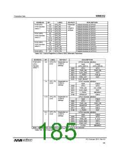
ADDRESS
BIT
LABEL
DEFAULT
DESCRIPTION
GPIOn debounce
R128 (80h)
12:0
GPn_DB [12:0]
1
GPIO de-
bounce
0 = GPIO is not debounced.
1 = GPIO is debounced (time from
GP_DBTIME[1:0])
R133 (85h)
7:6
GP_DBTIME
[1:0]
00
De-bounce time for all GPIO inputs
GPIO Control
00 = 64μs
01 = 0.5ms
10 = 1ms
11 = 4ms
Note: PWR_ON, PWR_OFF and
/WAKEUP have additional debounce
times.
Note: n is a number between 0 and 12 that identifies the individual GPIO.
Table 122 Configuring GPIO De-bounce
20.1.3 GPIO INTERRUPTS
The GPIO logic can raise a first-level interrupt, GPIO_INT (see Section 24). This interrupt is the
logical OR of the second-level GPIO interrupts described in Table 123.
ADDRESS
BIT
LABEL
DESCRIPTION
GPIOn interrupt.
R30 (1Eh)
12:0
GPn_EINT [12:0]
GPIO Interrupt
Status
(Trigger controlled by GPn registers.)
Note: This bit is cleared once read.
R38 (26h)
12:0
“IM_” + name of respective bit Mask bits for GPIO interrupts
in R30
GPIO Interrupt
Mask
Each of these bits masks the respective
bit in R30 when it is set to 1 (e.g.
GPn_EINT in R30 does not trigger a
GPIO_INT interrupt when IM_GPn_EINT
in R38 is set).
Note: n is a number between 0 and 12 that identifies the individual GPIO.
Table 123 GPIO Interrupts
PD, February 2011, Rev 4.4
181
w

 WOLFSON [ WOLFSON MICROELECTRONICS PLC ]