WM8352
Production Data
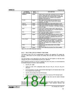
ALTERNATE
INPUT /
DESCRIPTION
FUNCTION NAME
OUTPUT
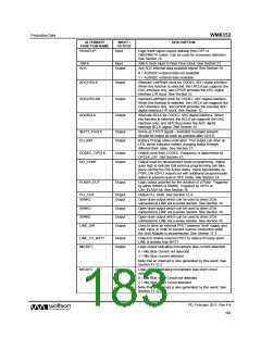
/MEMRST
Output
Output used to control other subsystems such as external
memory. Signal goes low to reset external memory. The
status of this signal in the Hibernate state is configurable,
allowing external memory contents to be retained in
Hibernate. See Section 14.
P_CLK
Output
1MHz output clock in phase with the internal DC-DC
converters. This signal can be used to sync external
circuits (e.g. DC-DCs).
POR_B
Output
Output
Output which toggles low to high during power-on reset
PWR_ON
Output used to indicate that device is powered on (eg. to
enable external DC-DC converters). This output is disabled
in the OFF state.
/RST
Output
Output used to indicate system resets. Signal goes low
during reset, same as the /RST pin. The pulse duration is
programmable. See Section 14.
RTC
Output
Output
Real Time Clock output - frequency is controlled by
RTC_DSW[3:0]. See Section 22.
SDOUT
4-wire Control Interface data output pin (SDOUT). Note
that this function is selected automatically on GPIO6 when
4-wire mode is selected, ie. regardless of the GP6_FN
control field. See Section 11.
/VCC_FAULT
Output
Indicates a fault condition on selectable DC Converters,
LDO Regulators and the Limit Switch. The mask bits in
Register 215 determine which supplies contribute to this
status flag. See Section 14.6.5, Section 14.7.3 and
Section 15.2.3.
VRTC
32kHz
Output
Output
Output from on-chip backup power source voltage
regulator VRTC.
32kHz clock output from the Real Time Clock oscillator.
Table 124 List of GPIO Alternate Functions
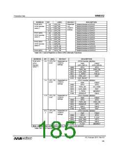
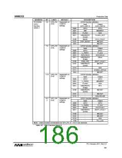
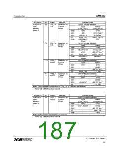
20.2.2 SELECTING GPIO ALTERNATE FUNCTIONS
The function of each GPIO pin is programmable by writing to the respective GPn register bits.
GPn_FN = 0000 selects the GPIO function and settings other than 0000 select various alternate
functions.
The GPIO function is also determined by the value of the GPn_DIR register bit. Note that, when
changing GPn_DIR, it is recommended to set GPn_FN = 0000 first.
When changing the function of a GPIO pin, (updating GPn_FN or GPn_DIR), it is recommended that
the following sequence of actions is taken sequentially.
.
.
Set GPn_FN = 0000
Update the other GPIO configuration fields GPn_DB, GPn_PU, GPn_PD, GPn_CFG,
GPn_DIR
.
If the new function is an input, ensure that the input trigger is in the inactive state (ie. logic
0 for a function that is active High)
.
.
.
Set GPn_FN according to the new GPIO function
Read the GPIO Interrupt Status Register R30 (1Eh) to clear any GPIO Interrupt events
If any bit in Register R30 (1Eh) was set when read, then read the System Interrupts
Register R24 (18h) to clear the IRQ pin
Note that GPIO7 is automatically enabled as CSB in 3-wire and 4-wire control modes. GPIO6 is
automatically enabled as SDOUT in 4-wire control mode. These automatic selections take
precedence over all other GPIO6 and GPIO7 control fields.
PD, February 2011, Rev 4.4
184
w

 WOLFSON [ WOLFSON MICROELECTRONICS PLC ]