Production Data
WM8352
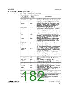
ALTERNATE
INPUT /
DESCRIPTION
FUNCTION NAME
OUTPUT
/WAKEUP
Input
Logic input signal causes wakeup from OFF or
HIBERNATE states. Can be used for accessory detection.
See Section 14.
32kHz
ADA
Input
32kHz clock input to Real Time Clock. See Section 22.
Aux ADC external data available signal. See Section 19.
0 = AUXADC external data not available
Output
1 = AUXADC external data available
ADCLRCLK
ADCLRCLKB
ADCBCLK
Output
Output
Output
Alternate Left/Right clock for CODEC ADC digital interface.
When this function is selected, the LRCLK pin supports the
DAC interface only, and GPIO5 provides the ADC digital
interface L/R clock. See Section 12.
Inverted Left/Right clock for CODEC ADC digital interface.
When this function is selected, the LRCLK pin supports the
DAC interface only, and GPIO6 provides the inverted ADC
digital interface L/R clock. See Section 12.
Alternate BCLK for CODEC ADC digital interface. When
this function is selected, the BCLK pin supports the DAC
interface only, and GPIO8 provides the ADC digital
interface BCLK signal. See Section 12.
/BATT_FAULT
CH_IND
Output
Output
Same as /UVLO signal – indicates no power present.
Should be output as soon as possible after /UVLO.
Battery Charge status indication. This output can drive an
LED, which indicates battery charging status through
different flash rates. See Section 17.
CODEC_OPCLK
DO_CONF
Output
Output
Output clock from CODEC. Frequency is determined by
OPCLK_DIV. See Section 12.
Output used for development mode programming. Signal
goes high to indicate that external programming can take
place (during the Pre-Active state). Same functionality as
PWR_ON (GPIO output) but with additional programmable
option to prevent reset in OFF mode. See Section 14.
FLASH_OUT
Output
Logic output asserted for the duration of a Flash. Triggered
by either SINKA or SINKB; Triggered by GPIO or
CSn_FLASH bit. See Section 16.
FLL_CLK
ISINKC
Output
Output
Output FLL clock. See Section 12.4.
Open-drain output which can be used to drive LEDs
connected to LINE via a series resistor. See Section 16.
ISINKD
ISINKE
Output
Output
Output
Open-drain output which can be used to drive LEDs
connected to LINE via a series resistor. See Section 16.
Open-drain output which can be used to drive LEDs
connected to LINE via a series resistor. See Section 16.
LINE_SW
Used to drive an external PFET between ‘Wall’ supply and
LINE input, in order to prevent reverse conduction when
the Wall Adapter is disconnected. See Section 17.1.
LINE_GT_BATT
MICDET
Output
Output
Output to enable external PFET to reduce IR loses when
LINE is greater than BATT
Logic output indicating microphone bias current detection.
0 = Mic Bias Current not detected
1 = Mic Bias Current detected
Note that an Interrupt is also generated by this event. See
Section 13.12.2.
MICSHT
Output
Logic output indicating microphone bias short circuit
detection.
0 = Mic Bias Short Circuit not detected
1 = Mic Bias Short Circuit detected
Note that an Interrupt is also generated by this event. See
Section 13.12.2.
PD, February 2011, Rev 4.4
183
w

 WOLFSON [ WOLFSON MICROELECTRONICS PLC ]