WM8352
Production Data
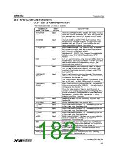
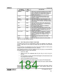
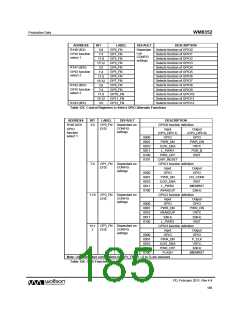
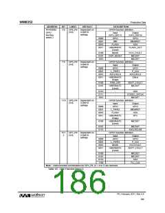
20.2 GPIO ALTERNATE FUNCTIONS
20.2.1 LIST OF ALTERNATE FUNCTIONS
The following alternate functions are available.
ALTERNATE
INPUT /
DESCRIPTION
FUNCTION NAME
OUTPUT
ADCLRCLK
Input
Alternate Left/Right clock for CODEC ADC digital interface.
When this function is selected, the LRCLK pin supports the
DAC interface only, and GPIO5 provides the ADC digital
interface L/R clock. See Section 12.
ADCBCLK
Input
Input
Alternate BCLK for CODEC ADC digital interface. When
this function is selected, the BCLK pin supports the DAC
interface only, and GPIO6 or GPIO8 provides the ADC
digital interface BCLK signal. See Section 12.
CHIP_RESET
Logic input to reset the Chip. When this input is asserted,
the chip performs a full reset and re-starts in accordance
with the current config mode settings.
Note that CHIP_RESET_ENA in register R3 should be set
to 1 when using CHIP_RESET as alternative GPIO
function.
CSB
Input
Input
Input
3-/4-wire Control Interface Chip Select pin (CSB). Note that
this function is selected automatically on GPIO7 when 3-/4-
wire mode is selected, ie. regardless of the GP7_FN
control field. See Section 11.
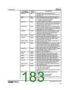
FLASH
Hardware trigger for flash function on ISINKA or ISINKB.
This function is rising edge triggered. The Current Sink
must be in Flash mode, and with the trigger set to GPIO.
See Section 16.
HIBERNATE
(Level)
Logic input to place the chip into hibernate. The behaviour
of some components of the WM8352 in Hibernate mode is
configurable. See Section 14.
This “level triggered” input is deemed to be asserted for as
long as it is logic 1 (or logic 0 if the polarity is inverted).
HIBERNATE
(Edge)
Input
Logic input to place the chip into hibernate. The behaviour
of some components of the WM8352 in Hibernate mode is
configurable. See Section 14.
When the “edge triggered” input is used, Hibernate is
selected when a rising edge occurs (or a falling edge if the
polarity is inverted). After Hibernate has been selected by
this method, a “StartUp” event (see Section 14.3.1) is
required to exit from Hibernate.
HEARTBEAT
Input
Input to Watchdog function, rising edge triggered. See
Section 23.
/LDO_ENA
L_PWR1
Input
Input
Enable signal for LDO1. See Section 14.7.4.
Logic input used to place DC-DC Converters or LDOs into
a Low Power state. See Section 14.
L_PWR2
L_PWR3
MASK
Input
Input
Input
Logic input used to place DC-DC Converters or LDOs into
a Low Power state. See Section 14.
Logic input used to place DC-DC Converters or LDOs into
a Low Power state. See Section 14.
Mask input to AUXADC. This input may be used either to
block all inputs to the AUXADC, or to initiate A-D
Conversions. See Section 19.
/MR
Input
Logic input used to drive the /RST pin and the /RST and
/MEMRST (GPIO outputs) low. Note that this input has no
other effect on internal circuits. See Section 14.
PWR_OFF
PWR_ON
Input
Input
Logic input signal causes a controlled shutdown of the
WM8352. See Section 14.
Power on input signal from processor (input switching
threshold 1.0V). See Section 14.
PD, February 2011, Rev 4.4
182
w

 WOLFSON [ WOLFSON MICROELECTRONICS PLC ]