Production Data
WM8352
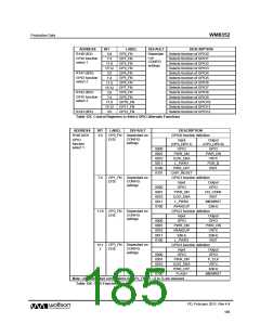
ADDRESS
BIT
3:0
LABEL
GP0_FN
DEFAULT
DESCRIPTION
R140 (8Ch
Dependan
t on
CONFIG
settings
Selects function of GPIO0
Selects function of GPIO1
Selects function of GPIO2
Selects function of GPIO3
Selects function of GPIO4
Selects function of GPIO5
Selects function of GPIO6
Selects function of GPIO7
Selects function of GPIO8
Selects function of GPIO9
Selects function of GPIO10
Selects function of GPIO11
Selects function of GPIO12
GPIO function
select 1
7:4
11:8
15:12
3:0
GP1_FN
GP2_FN
GP3_FN
GP4_FN
GP5_FN
GP6_FN
GP7_FN
GP8_FN
GP9_FN
GP10_FN
GP11_FN
GP12_FN
R141 (8Dh)
GPIO function
select 2
7:4
11:8
15:12
3:0
R142 (8Eh)
GPIO function
select 3
7:4
11:8
15:12
3:0
R143 (8Fh)
Table 125 Control Registers to Select GPIO Alternate Functions
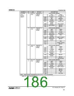
ADDRESS
BIT
LABEL
DEFAULT
DESCRIPTION
R140 (8Ch
3:0
GP0_FN Dependant on
GPIO0 function definition
[3:0]
CONFIG
settings
GPIO
function
select 1
Input
(GPn_DIR=1)
Output
(GPn_DIR=0)
0000
0001
0010
0011
0100
0101
GPIO
GPIO
PWR_ON
/LDO_ENA
L_PWR1
PWR_ON
VRTC
POR_B
/RST
PWR_OFF
CHIP_RESET
7:4
GP1_FN Dependant on
GPIO1 function definition
[3:0]
CONFIG
settings
Input
Output
0000
0001
0010
0011
0100
GPIO
GPIO
DO_CONF
/RST
PWR_ON
/LDO_ENA
L_PWR2
/WAKEUP
/MEMRST
32kHz
11:8 GP2_FN Dependant on
GPIO2 function definition
[3:0]
CONFIG
settings
Input
GPIO
Output
0000
0001
0010
0011
0100
GPIO
PWR_ON
VRTC
PWR_ON
/WAKEUP
32kHz
32kHz
L_PWR3
/RST
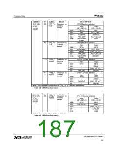
15:1 GP3_FN Dependant on
GPIO3 function definition
2
[3:0]
CONFIG
settings
Input
Output
0000
0001
0010
0011
0100
GPIO
GPIO
P_CLK
VRTC
PWR_ON
/LDO_ENA
PWR_OFF
FLASH
32kHz
/MEMRST
Note: Undocumented combinations for GPn_FN (n = 0 to 3) are reserved
Table 126 GPIO Function Select 1
PD, February 2011, Rev 4.4
185
w

 WOLFSON [ WOLFSON MICROELECTRONICS PLC ]