W90N745CD/W90N745CDG
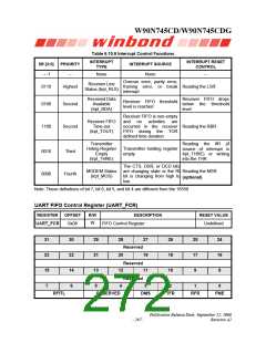
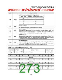
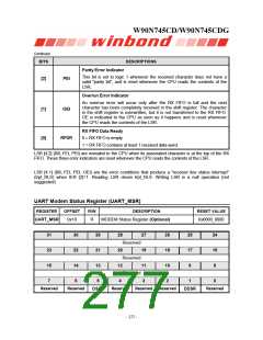
BITS
[7:6]
DESCRIPTIONS
RX FIFO Interrupt (Irpt_RDA) Trigger Level
RFITL [7:6]
Irpt_RDA Trigger Level (Bytes)
01
04
08
14
00
01
10
11
RFITL
DMA Mode Select
DMS
TFR
[3]
[2]
The DMA function is not implemented in this version.
TX FIFO Reset
Setting this bit will generate an OSC cycle reset pulse to reset TX FIFO. The
TX FIFO becomes empty (TX pointer is reset to 0) after such reset. This bit is
returned to 0 automatically after the reset pulse is generated.
RX FIFO Reset
Setting this bit will generate an OSC cycle reset pulse to reset RX FIFO. The
RX FIFO becomes empty (RX pointer is reset to 0) after such reset. This bit
is returned to 0 automatically after the reset pulse is generated.
RFR
FME
[1]
[0]
FIFO Mode Enable
Because UART is always operating in the FIFO mode, writing this bit has no
effect while reading always gets logical one. This bit must be 1 when other
FCR bits are written to; otherwise, they will not be programmed.
UART Line Control Register (UART_LCR)
REGISTER
OFFSET
R/W
DESCRIPTION
Line Control Register
RESET VALUE
R/W
UART_LCR
0x0C
0x0000_0000
31
23
15
30
22
14
29
28
20
12
4
27
19
11
26
18
10
25
17
9
24
16
8
Reserved
21
13
Reserved
Reserved
7
6
5
3
2
1
0
DLAB
BCB
SPE
EPE
PBE
NSB
WLS
- 268 -

 WINBOND [ WINBOND ]