UCC21759-Q1
SLUSEB4A – AUGUST 2020 – REVISED DECEMBER 2020
www.ti.com
ROH_EFF
2 ROH_EFF + RON + RG _Int ROL +ROFF +RG _Int
ROL
1
P
=
∂(
+
)∂(VDD - VEE)∂ fsw ∂Qg = 0.505W
SW
(6)
Thus, the total power loss is:
P =P +P = 0.10W +0.505W = 0.605W
DR
Q
SW
(7)
When the board temperature is 125°C, the junction temperature can be estimated as:
Tj = T + yjb ∂P ö 150oC
b
DR
(8)
Therefore, for the application in this example, with 125°C board temperature, the maximum switching frequency
is ~50kHz to keep the gate driver in the thermal limit. By using a lower switching frequency, or increasing
external gate resistance, the gate driver can be operated at a higher switching frequency.
9.2.2.6 Desaturation (DESAT) Protection
A standard desaturation circuit can be applied to the DESAT pin. If the voltage of the DESAT pin is higher than
the threshold VDESAT, the soft turn-off is initiated. A fault will be reported to the input side to DSP/MCU. The
output is held to LOW after the fault is detected, and can only be reset by the RST/EN pin. The state-of-art
overcurrent and short circuit detection time helps to ensure a short shutdown time for SiC MOSFET and IGBT.
If DESAT pin is not in use, it must be tied to COM to avoid overcurrent fault false triggering.
•
Fast reverse recovery high voltage diode is recommended in the desaturation circuit. A resistor is
recommended in series with the high voltage diode to limit the inrush current. Multiple high voltage diodes
can be placed in series to reduce the DESAT detection voltage as seen by the IGBT or SiC MOSFET based
on the forward voltage drop.
•
•
A Schottky diode is recommended from COM to DESAT to prevent driver damage caused by negative
voltage.
A Zener diode is recommended from COM to DESAT to prevent driver damage caused by positive voltage.
9.2.2.7 Isolated Analog Signal Sensing
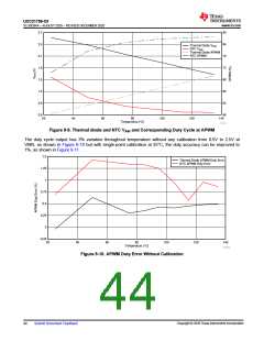
The isolated analog signal sensing feature provides a simple isolated channel for the isolated temperature
detection, voltage sensing and etc. One typical application of this function is the temperature monitor of the
power semiconductor. Thermal diodes or temperature sensing resistors are integrated in the SiC MOSFET or
IGBT module close to the dies to monitor the junction temperature. UCC21759-Q1 has an internal 200uA current
source with ±3% accuracy across temperature, which can forward bias the thermal diodes or create a voltage
drop on the temperature sensing resistors. The sensed voltage from the AIN pin is passed through the isolation
barrier to the input side and transformed to a PWM signal. The duty cycle of the PWM changes linearly from
10% to 88% when the AIN voltage changes from 4.5V to 0.6V and can be represented using Equation 9.
DAPWM(%) = -20 * VAIN +100
(9)
9.2.2.7.1 Isolated Temperature Sensing
A typical application circuit is shown in Figure 9-7. To sense temperature, the AIN pin is connected to the thermal
diode or thermistor which can be discrete or integrated within the power module. A low pass filter is
recommended for the AIN input. Since the temperature signal does not have a high bandwidth, the low pass
filter is mainly used for filtering the noise introduced by the switching of the power device, which does not require
stringent control for propagation delay. The filter capacitance for Cfilt can be chosen between 1nF to 100nF and
the filter resistance Rfilt between 1Ω to 10Ω according to the noise level.
The output of APWM is directly connected to the microcontroller to measure the duty cycle dependent on the
voltage input at AIN, using Equation 9.
Copyright © 2020 Texas Instruments Incorporated
42
Submit Document Feedback

 TI [ TEXAS INSTRUMENTS ]