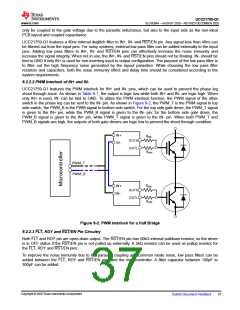
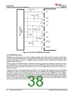
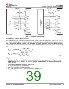
UCC21759-Q1
SLUSEB4A – AUGUST 2020 – REVISED DECEMBER 2020
www.ti.com
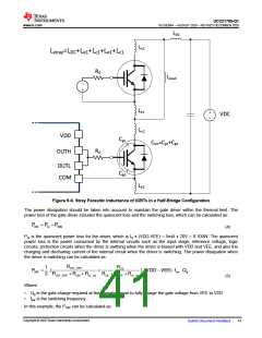
LDC
Lc1
Lstray=LDC+Le1+Lc1+Le1+Lc1
RG
Lload
t
+
Le1
+
VDC
t
Lc2
VDD
Cgc
Cies=Cgc+Cge
RG
OUTH
OUTL
COM
Cge
Le2
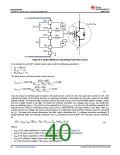
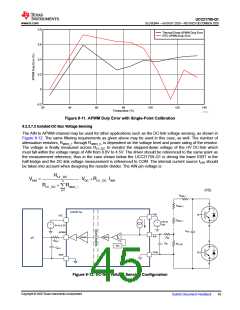
Figure 9-6. Stray Parasitic Inductance of IGBTs in a Half-Bridge Configuration
The power dissipation should be taken into account to maintain the gate driver within the thermal limit. The
power loss of the gate driver includes the quiescent loss and the switching loss, which can be calculated as:
P
= PQ +P
DR
SW
(4)
PQ is the quiescent power loss for the driver, which is Iq x (VDD-VEE) = 5mA x 20V = 0.100W. The quiescent
power loss is the power consumed by the internal circuits such as the input stage, reference voltage, logic
circuits, protection circuits when the driver is swithing when the driver is biased with VDD and VEE, and also the
charging and discharing current of the internal circuit when the driver is switching. The power dissipation when
the driver is switching can be calculated as:
ROH_EFF
2 ROH_EFF +RON +RG _Int ROL +ROFF +RG _Int
ROL
1
P
=
∂(
+
)∂(VDD - VEE)∂ fsw ∂Qg
SW
(5)
Where
•
•
Qg is the gate charge required at the operation point to fully charge the gate voltage from VEE to VDD
fsw is the switching frequency
In this example, the PSW can be calculated as:
Copyright © 2020 Texas Instruments Incorporated
Submit Document Feedback
41

 TI [ TEXAS INSTRUMENTS ]