UCC21759-Q1
SLUSEB4A – AUGUST 2020 – REVISED DECEMBER 2020
www.ti.com
3.3V to 5V
VCC
15
9
1µF
0.1µF
GND
IN+
10
INt
11
5kQ
5kQ 5kQ
FLT
12
13
100pF
RDY
100pF
RST/EN
14
16
100pF
APWM
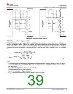
Figure 9-3. FLT, RDY and RST/EN Pins Circuitry
9.2.2.4 RST/EN Pin Control
RST/EN pin has two functions. It is used to enable or shutdown the outputs of the driver and to reset the fault
signaled on the FLT pin after DESAT is detected. RST/EN pin needs to be pulled up to enable the device; when
the pin is pulled down, the device is in disabled status. By default the driver is disabled with the internal 50kΩ
pulldown resistor at this pin.
When the driver is latched after DESAT is detected, the FLT pin and output are latched low and need to be reset
by the RST/EN pin. The microcontroller must send a signal to RST/EN pin after the fault to reset the driver. The
driver will not respond until after the mute time tFLTMUTE. The reset signal must be held low for at least tRSTFIL
after the mute time.
This pin can also be used to automatically reset the driver. The continuous input signal IN+ or IN- can be applied
to RST/EN pin. There is no separate reset signal from the microcontroller when configuring the driver this way. If
the PWM is applied to the non-inverting input IN+, then IN+ can also be tied to RST/EN pin. If the PWM is
applied to the inverting input IN-, then a NOT logic is needed between the PWM signal from the microcontroller
and the RST/EN pin. Using either configuration results in the driver being reset in every switching cycle without
an extra control signal from microcontroller tied to RST/EN pin. One must ensure the PWM off-time is greater
than tRSTFIL in order to reset the driver in cause of a DESAT fault.
Copyright © 2020 Texas Instruments Incorporated
38
Submit Document Feedback

 TI [ TEXAS INSTRUMENTS ]