UCC21759-Q1
SLUSEB4A – AUGUST 2020 – REVISED DECEMBER 2020
www.ti.com
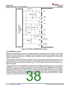
3.3V to 5V
0.1µF
3.3V to 5V
VCC
VCC
15
15
1µF
1µF
0.1µF
GND
IN+
GND
IN+
9
9
10
10
INt
INt
5kQ
11
5kQ
5kQ
11
5kQ
FLT
FLT
12
13
12
13
100pF
100pF
100pF
100pF
RDY
RDY
RST/EN
APWM
RST/EN
APWM
14
16
14
16
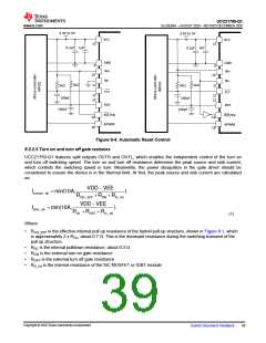
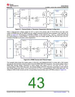
Figure 9-4. Automatic Reset Control
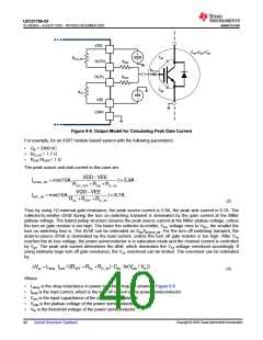
9.2.2.5 Turn on and turn off gate resistors
UCC21759-Q1 features split outputs OUTH and OUTL, which enables the independent control of the turn on
and turn off switching speed. The turn on and turn off resistance determine the peak source and sink current,
which controls the switching speed in turn. Meanwhile, the power dissipation in the gate driver should be
considered to ensure the device is in the thermal limit. At first, the peak source and sink current are calculated
as:
VDD - VEE
ROH_EFF +RON +RG _Int
Isource _ pk = min(10A,
)
VDD - VEE
ROL +ROFF +RG _Int
Isink _ pk = min(10A,
)
(1)
Where
•
ROH_EFF is the effective internal pull up resistance of the hybrid pull-up structure, shown in Figure 8-1, which
is approximately 2 x ROL, about 0.7 Ω. This is the dominant resistance during the switching transient of the
pull up structure.
•
•
•
•
ROL is the internal pulldown resistance, about 0.3 Ω
RON is the external turn on gate resistance
ROFF is the external turn off gate resistance
RG_Int is the internal resistance of the SiC MOSFET or IGBT module
Copyright © 2020 Texas Instruments Incorporated
Submit Document Feedback
39

 TI [ TEXAS INSTRUMENTS ]