UCC21759-Q1
SLUSEB4A – AUGUST 2020 – REVISED DECEMBER 2020
www.ti.com
VDD
Cies=Cgc+Cge
+
Cgc
VDD
ROH_EFF
OUTH
t
RON
RG_Int
OUTL
ROFF
Cge
+
VEE
ROL
t
VEE
COM
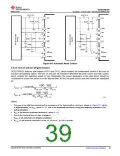
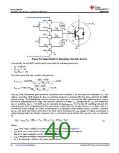
Figure 9-5. Output Model for Calculating Peak Gate Current
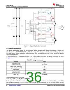
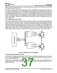
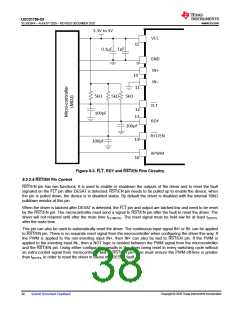
For example, for an IGBT module based system with the following parameters:
•
•
•
Qg = 3300 nC
RG_Int = 1.7 Ω
RON=ROFF= 1 Ω
The peak source and sink current in this case are:
VDD - VEE
ROH_EFF +RON +RG _Int
Isource _ pk = min(10A,
) ö 5.9A
VDD - VEE
ROL +ROFF +RG _Int
Isink _ pk = min(10A,
) ö 6.7A
(2)
Thus by using 1Ω external gate resistance, the peak source current is 5.9A, the peak sink current is 6.7A. The
collector-to-emitter dV/dt during the turn on switching transient is dominated by the gate current at the Miller
plateau voltage. The hybrid pullup structure ensures the peak source current at the Miller plateau voltage, unless
the turn on gate resistor is too high. The faster the collector-to-emitter, Vce, voltage rises to VDC, the smaller the
turn on switching loss is. The dV/dt can be estimated as Qgc/Isource_pk. For the turn off switching transient, the
drain-to-source dV/dt is dominated by the load current, unless the turn off gate resistor is too high. After Vce
reaches the dc bus voltage, the power semiconductor is in saturation mode and the channel current is controlled
by Vge. The peak sink current determines the dI/dt, which dominates the Vce voltage overshoot accordingly. If
using relatively large turn off gate resistance, the Vce overshoot can be limited. The overshoot can be estimated
by:
DV = Lstray ∂Iload / ((ROFF +ROL +RG_Int )∂Cies ∂ln(Vplat / V ))
ce
th
(3)
Where
•
•
•
•
•
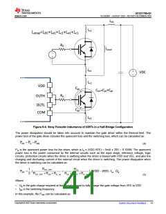
Lstray is the stray inductance in power switching loop, as shown in Figure 9-6
Iload is the load current, which is the turn off current of the power semiconductor
Cies is the input capacitance of the power semiconductor
Vplat is the plateau voltage of the power semiconductor
Vth is the threshold voltage of the power semiconductor
Copyright © 2020 Texas Instruments Incorporated
40
Submit Document Feedback

 TI [ TEXAS INSTRUMENTS ]