UCC21759-Q1
SLUSEB4A – AUGUST 2020 – REVISED DECEMBER 2020
www.ti.com
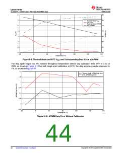
0.8
Thermal Diode APWM Duty Error
NTC APWM Duty Error
0.6
0.4
0.2
0
-0.2
20
40
60
80
Temperature (èC)
100
120
140
APWM
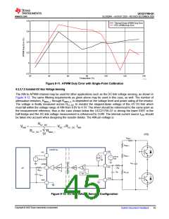
Figure 9-11. APWM Duty Error with Single-Point Calibration
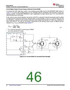
9.2.2.7.2 Isolated DC Bus Voltage Sensing
The AIN to APWM channel may be used for other applications such as the DC-link voltage sensing, as shown in
Figure 9-12. The same filtering requirements as given above may be used in this case, as well. The number of
attenuation resistors, Ratten_1 through Ratten_n, is dependent on the voltage level and power rating of the resistor.
The voltage is finally measured across RLV_DC to monitor the stepped-down voltage of the HV DC-link which
must fall within the voltage range of AIN from 0.6V to 4.5V. The driver should be referenced to the same point as
the measurement reference, thus in the case shown below the UCC21759-Q1 is driving the lower IGBT in the
half-bridge and the DC-link voltage measurement is referenced to COM. The internal current source IAIN should
be taken into account when designing the resistor divider. The AIN pin voltage is:
RLV _DC
n
VAIN
=
∂ VDC +RLV _DC ∂IAIN
RLV _DC
+
R
atten _ i
ƒ
i=1
(10)
Ratten_1
Ratten_2
UCC217xx
VDD
VCC
Ratten_n
13V to
33V
+
+
3V to 5.5V
APWM
œ
œ
CDC
+
AIN
DEMOD
MOD
µC
Rfilt
Cfilt
Rfilt_2
Cfilt_2
GND
RLV_DC
OSC
COM
Figure 9-12. DC-link Voltage Sensing Configuration
Copyright © 2020 Texas Instruments Incorporated
Submit Document Feedback
45

 TI [ TEXAS INSTRUMENTS ]