TPS929160-Q1
ZHCSNG0 – APRIL 2023
www.ti.com.cn
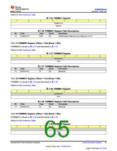
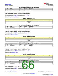
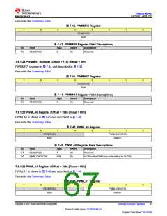
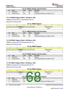
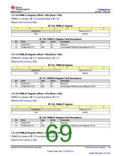
7.6.1.30 PWMLC1 Register (Offset = 25h) [Reset = 00h]
PWMLC1 is shown in 图 7-50 and described in 表 7-50.
Return to the Summary Table.
图 7-50. PWMLC1 Register
7
6
5
4
3
2
1
0
0
0
RESERVED
R-0h
PWMLOWOUTC1
R/W-0h
表 7-50. PWMLC1 Register Field Descriptions
Bit
Field
Type
Reset
Description
7-4
3-0
RESERVED
R
0h
Reserved
PWMLOWOUTC1
R/W
0h
4-LSB output PWM duty-cycle setting for OUTC1
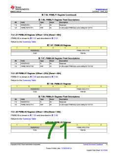
7.6.1.31 PWMLD0 Register (Offset = 26h) [Reset = 00h]
PWMLD0 is shown in 图 7-51 and described in 表 7-51.
Return to the Summary Table.
图 7-51. PWMLD0 Register
7
6
5
4
3
2
1
RESERVED
R-0h
PWMLOWOUTD0
R/W-0h
表 7-51. PWMLD0 Register Field Descriptions
Bit
Field
Type
Reset
Description
7-4
3-0
RESERVED
R
0h
Reserved
PWMLOWOUTD0
R/W
0h
4-LSB output PWM duty-cycle setting for OUTD0
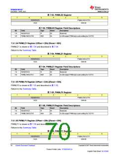
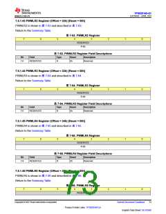
7.6.1.32 PWMLD1 Register (Offset = 27h) [Reset = 00h]
PWMLD1 is shown in 图 7-52 and described in 表 7-52.
Return to the Summary Table.
图 7-52. PWMLD1 Register
7
6
5
4
3
2
1
RESERVED
R-0h
PWMLOWOUTD1
R/W-0h
表 7-52. PWMLD1 Register Field Descriptions
Bit
Field
Type
Reset
Description
7-4
3-0
RESERVED
R
0h
Reserved
PWMLOWOUTD1
R/W
0h
4-LSB output PWM duty-cycle setting for OUTD1
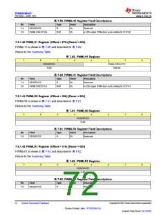
7.6.1.33 PWMLE0 Register (Offset = 28h) [Reset = 00h]
PWMLE0 is shown in 图 7-53 and described in 表 7-53.
Return to the Summary Table.
Copyright © 2023 Texas Instruments Incorporated
Submit Document Feedback
69
Product Folder Links: TPS929160-Q1
English Data Sheet: SLVSG60

 TI [ TEXAS INSTRUMENTS ]