TPS929160-Q1
ZHCSNG0 – APRIL 2023
www.ti.com.cn
Return to the Summary Table.
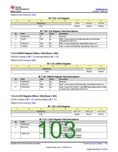
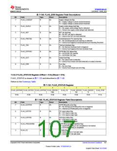
图 7-123. CLR Register
7
6
5
4
3
2
1
0
RESERVED
R-0h
CLRFS
R/W-0h
CLRFAULT
R/W-0h
CLRPOR
R/W-0h
表 7-129. CLR Register Field Descriptions
Bit
Field
Type
Reset
Description
7-3
2
RESERVED
CLRFS
R
0h
Reserved
R/W
0h
Write 1 to force device to exit fail-safe state to normal state,
automatically returns to 0
1
0
CLRFAULT
CLRPOR
R/W
R/W
0h
0h
Write 1 to clear all fault flags, automatically returns to 0
Write 1 to clear POR fault flag, automatically returns to 0
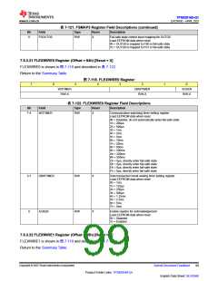
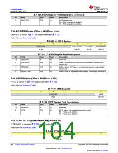
7.6.4.3 DEBUG Register (Offset = 92h) [Reset = 00h]
DEBUG is shown in 图 7-124 and described in 表 7-130.
Return to the Summary Table.
图 7-124. DEBUG Register
7
6
5
4
3
2
1
0
RESERVED
R-0h
FORCEFS
R/W-0h
FPRCEERR
R/W-0h
表 7-130. DEBUG Register Field Descriptions
Bit
Field
Type
Reset
Description
7-2
1
RESERVED
FORCEFS
FPRCEERR
R
0h
Reserved
R/W
R/W
0h
Write 1 to force device to fail-safe state, automatically returns to 0
0
0h
Write 1 to set FLAG_ERR to 1 and ERR output pulled down for 50µs
in normal state, automatically returns to 0
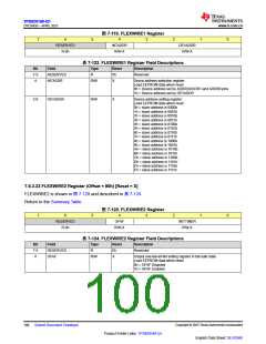
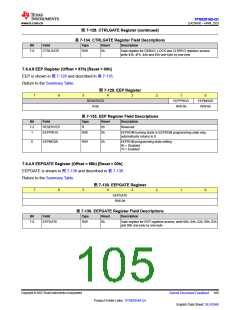
7.6.4.4 LOCK Register (Offset = 93h) [Reset = 03h]
LOCK is shown in 图 7-125 and described in 表 7-131.
Return to the Summary Table.
图 7-125. LOCK Register
7
6
5
4
3
2
1
0
RESERVED
R-0h
BRTLOCK
R/W-0h
CONFLOCK
R/W-1h
IOUTLOCK
R/W-1h
表 7-131. LOCK Register Field Descriptions
Bit
Field
Type
Reset
Description
7-3
2
RESERVED
BRTLOCK
R
0h
Reserved
R/W
0h
BRT register lock
0h = Write protection is disabled
1h = Write protection is enabled
1
CONFLOCK
R/W
1h
CONF register lock
0h = Write protection is disabled
1h = Write protection is enabled
Copyright © 2023 Texas Instruments Incorporated
Submit Document Feedback 103
Product Folder Links: TPS929160-Q1
English Data Sheet: SLVSG60

 TI [ TEXAS INSTRUMENTS ]