TPS929160-Q1
ZHCSNG0 – APRIL 2023
www.ti.com.cn
表 7-121. FSMAP3 Register Field Descriptions (continued)
Bit
Field
FSOUTG0
Type
Reset
Description
0
R/W
X
Fail-safe state control input mapping for OUTG0
Load EEPROM data when reset
0h = OUTG0 is mapped to FS0 in fail-safe state
1h = OUTG0 is mapped to FS1 in fail-safe state
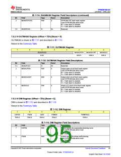
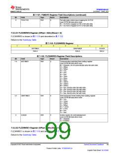
7.6.3.21 FLEXWIRE0 Register (Offset = 84h) [Reset = X]
FLEXWIRE0 is shown in 图 7-118 and described in 表 7-122.
Return to the Summary Table.
图 7-118. FLEXWIRE0 Register
7
6
5
4
3
2
1
0
WDTIMER
R/W-X
DBWTIMER
R/W-X
ACKEN
R/W-X
表 7-122. FLEXWIRE0 Register Field Descriptions
Bit
Field
Type
Reset
Description
7-4
WDTIMER
R/W
X
Communication watchdog timer setting register
Load EEPROM data when reset
0h = Disabled, do not automatically enter fail-safe state
1h = 200µs
2h = 500µs
3h = 1ms
4h = 2ms
5h = 5ms
6h = 10ms
7h = 20ms
8h = 50ms
9h = 100ms
Ah = 200ms
Bh = 500ms
Ch = 0µs, directly enter fail-safe state
Dh = 0µs, directly enter fail-safe state
Eh = 0µs, directly enter fail-safe state
Fh = 0µs, directly enter fail-safe state
3-1
DBWTIMER
R/W
X
Data transaction break waiting timer setting register
Load EEPROM data when reset
0h = 1ms
1h = 125µs
2h = 250µs
3h = 500µs
4h = 1.25ms
5h = 2.5ms
6h = 5ms
7h = 5ms
0
ACKEN
R/W
X
Enable register for acknowledgement
Load EEPROM data when reset
0h = Disabled
1h = Enabled
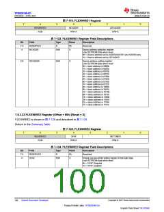
7.6.3.22 FLEXWIRE1 Register (Offset = 85h) [Reset = X]
FLEXWIRE1 is shown in 图 7-119 and described in 表 7-123.
Return to the Summary Table.
Copyright © 2023 Texas Instruments Incorporated
Submit Document Feedback
99
Product Folder Links: TPS929160-Q1
English Data Sheet: SLVSG60

 TI [ TEXAS INSTRUMENTS ]