TPS929160-Q1
ZHCSNG0 – APRIL 2023
www.ti.com.cn
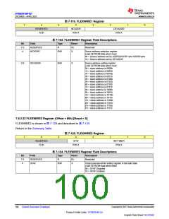
7.6.4 CTRL Registers
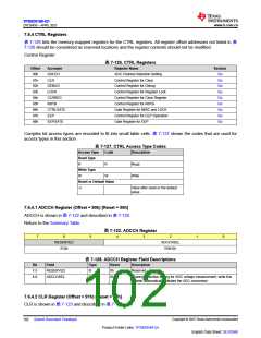
表 7-126 lists the memory-mapped registers for the CTRL registers. All register offset addresses not listed in 表
7-126 should be considered as reserved locations and the register contents should not be modified.
Control Register
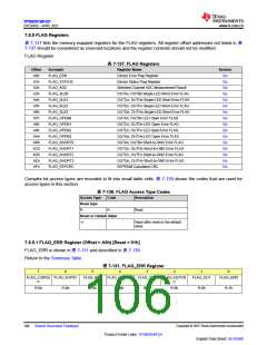
表 7-126. CTRL Registers
Offset
90h
91h
92h
93h
94h
95h
96h
97h
98h
Acronym
ADCCH
CLR
Register Name
Section
Go
ADC Channel Selection Setting
Control Register for Clear
Go
DEBUG
LOCK
Control Register for Debug
Control Register for Register Lock
Control Register for Clear Register
Control Register for NSTB
Gate Register for MISC and LOCK
Control Register for EEP Operation
Gate Register for EEP
Go
Go
CLRREG
NSTB
Go
Go
CTRLGATE
EEP
Go
Go
EEPGATE
Go
Complex bit access types are encoded to fit into small table cells. 表 7-127 shows the codes that are used for
access types in this section.
表 7-127. CTRL Access Type Codes
Access Type
Read Type
R
Code
Description
R
Read
Write Type
W
W
Write
Reset or Default Value
-n
Value after reset or the default
value
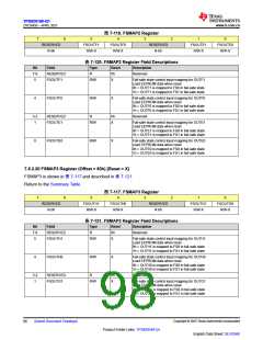
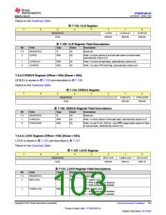
7.6.4.1 ADCCH Register (Offset = 90h) [Reset = 00h]
ADCCH is shown in 图 7-122 and described in 表 7-128.
Return to the Summary Table.
图 7-122. ADCCH Register
7
6
5
4
3
2
1
0
RESERVED
R-0h
ADCCHSEL
R/W-0h
表 7-128. ADCCH Register Field Descriptions
Bit
Field
Type
Reset
Description
7-5
4-0
RESERVED
ADCCHSEL
R
0h
Reserved
R/W
0h
Channel selection setting for ADC voltage measurement, write this
register automatically initiates the ADC conversion
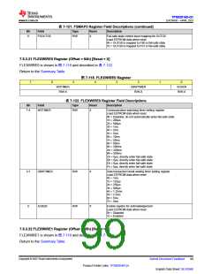
7.6.4.2 CLR Register (Offset = 91h) [Reset = 00h]
CLR is shown in 图 7-123 and described in 表 7-129.
Copyright © 2023 Texas Instruments Incorporated
102 Submit Document Feedback
Product Folder Links: TPS929160-Q1
English Data Sheet: SLVSG60

 TI [ TEXAS INSTRUMENTS ]