TPS65163
www.ti.com
SLVSA28 –OCTOBER 2009
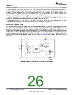
VSWB
RFLY
CFLY
VGL
-
CTRLN
COUT
+
CCOLLECTOR
RPULL-DOWN
ICTRLN
R1
FBN
R2
RFILTER
VLOGIC
CFILTER
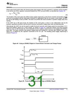
Figure 45. Negative Charge Pump Application Circuit
The TPS65163 contains a circuit to protect the negative charge pump against short circuits on its output. A
short-circuit condition is detected as long as the FBN pin remains above 1.65 V, during which time the charge
pump output current is limited.
To ensure proper start-up under normal conditions, circuit designers should make sure the full load current is not
drawn by the load until the feedback voltage VFBN is below the short-circuit threshold voltage. The value of VGL
beyond which the negative charge pump no longer works in short-circuit mode is given by Equation 23.
æ
R1 ö
VGL(SC) = -1.65 V ´ 1-
ç
÷
R2 ø
è
(23)
NEGATIVE CHARGE PUMP DESIGN PROCEDURE
Setting the Output Voltage (Negative Charge Pump)
The negative charge pump output voltage is programmed by a resistor divider according to Equation 24.
R1
VGL = - VLOGIC ´
R2
(24)
(25)
Rearranging Equation 25, the values of R1 and R2 are calculated.
VGL
R1 = R2
´
V
LOGIC
A current of the order of 1 mA through the resistor network ensures accuracy and increases the circuit's immunity
to noise. It also ensures a minimum load on the charge pump, which reduces output voltage ripple under no-load
conditions. A good approach is to assume a value of about 3.3 kΩ for the lower resistor (R2) and then select the
upper resistor (R1) to set the desired output voltage.
Note that the maximum voltage in an application is determined by the boost converter output voltage and the
voltage drop across the diodes and NPN transistor. For a typical application in which the negative charge pump
is configured as a voltage inverter, the maximum (i.e., most negative) output voltage is given by Equation 26.
VGL(MAX) = -V + 2 ´ V + V
)
(
IN
F
CE
(26)
where VF is the forward voltage of each diode and VCE is the collector-emitter voltage of the NPN transistor
(recommended to be at least 1 V to avoid transistor saturation).
Copyright © 2009, Texas Instruments Incorporated
Submit Documentation Feedback
27
Product Folder Link(s) :TPS65163

 TI [ TEXAS INSTRUMENTS ]