TPS65163
www.ti.com
SLVSA28 –OCTOBER 2009
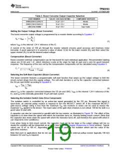
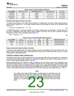
Table 4. Buck Converter Inductor Selection
PART NUMBER
INDUCTOR VALUE
COMPONENT SUPPLIER
SIZE (L×W×H, mm)
ISAT / DCR
4 A / 29 mΩ
3 A / 38 mΩ
4.8 A / 26 mΩ
4 A / 28 mΩ
CDRH8D43
CDRH8D38
MSS 1048-103
744066100
10 µH
10 µH
10 µH
10 µH
Sumida
Sumida
Coilcraft
Wuerth
8.3 × 8.3 × 4.5
8.3 × 8.3 × 4
10.5 × 10.5 × 5.1
10 × 10 × 3.8
Rectifier Diode Selection (Buck Converter)
To achieve good efficiency, the rectifier diode should be a Schottky type. Its reverse voltage rating should be
higher than the maximum VIN. The average rectified forward current through the diode can be calculated using
Equation 15.
IRECT(AVG) = ILOGIC(EFFECTIVE)
´ 1 - D
(
)
(15)
A Schottky diode with a 2-A average rectified current rating is adequate for most applications. Smaller diodes can
be used in applications with lower output current; however, the diode must be able to handle the power
dissipated in it, which can be calculated using Equation 16.
PRECT = IRECT(AVG) ´ VF
(16)
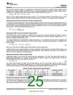
Table 5. Buck Converter Rectifier Diode Selection
PART NUMBER
MBRS320
SL22
VR / IAVG
20 V / 3 A
20 V / 2 A
20 V / 2 A
VF
RθJA
SIZE
SMC
SMB
SMB
COMPONENT SUPPLIER
International Rectifier
0.44 V at 3 A
0.44 V at 2 A
0.5 V at 2 A
46°C/W
75°C/W
75°C/W
Vishay Semiconductor
Fairchild Semiconductor
SS22
Output Capacitance Selection (Buck Converter)
To minimize output voltage ripple, the output capacitors should be good-quality ceramic types with low ESR. The
buck converter is stable over a range of output capacitance values, but an output capacitance of 44 µF is a good
starting point for typical applications.
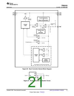
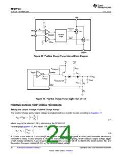
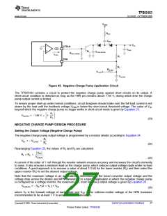
POSITIVE CHARGE PUMP CONTROLLER
The positive charge pump is driven directly from the boost converter switch node and regulated by controlling the
current through an external PNP transistor. An internal block diagram of the positive charge pump is shown in
Figure 42 and a typical application circuit in Figure 43.
During normal operation, the TPS65163 is able to provide up to 5 mA of base current and is designed to work
best with transistors whose dc gain (hFE) is between 100 and 300. The charge pump is protected against short
circuits on its output, which are detected when the voltage on the charge pump feedback pin (VFBP) is below
100 mV. During short-circuit mode, the base current available from the CTRLP pin is limited to 55 µA. Note that if
a short circuit is detected during normal operation, boost converter switching is also halted until VFBP > 100 mV.
NOTE
The emitter of the external PNP transistor should always be connected to VS, the
output of the boost converter at the output side of the isolation switch. The TPS65163
uses the CTRLP pin to sense the voltage across the isolation switch and control boost
converter start-up. Connecting the emitter of the external PNP transistor to any other
voltage (e.g., VIN) prevents proper start-up of the boost converter and positive charge
pump.
Copyright © 2009, Texas Instruments Incorporated
Submit Documentation Feedback
23
Product Folder Link(s) :TPS65163

 TI [ TEXAS INSTRUMENTS ]