TPS65163
www.ti.com
SLVSA28 –OCTOBER 2009
Reset pulse timing starts when the internal power-good signal of the buck converter is asserted, and its duration
is set by the size of the capacitor connected between the CRST pin and AGND, as described by Equation 30.
CRST ´ VREF
tRST
=
IRST
(30)
The duration of the reset pulse also affects power-supply sequencing, as the boost converter and positive charge
pump are not enabled until the reset pulse is finished. In applications that do not require a reset signal, the RST
pin can be left floating or tied to AGND. This does not prevent the boost converter or positive charge pump from
starting.
If the CRST pin is left open-circuit, the duration of the reset pulse is close to zero (determined only by the
parasitic capacitance present), and the boost converter and positive charge pump start up instantaneously.
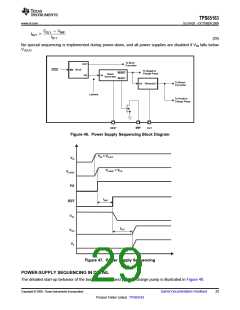
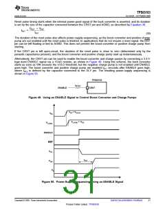
Alternatively, the CRST pin can be used to enable the boost converter and charge pumps by connecting a 3.3-V
logic-level ENABLE signal via a 10-kΩ resistor, as shown in Figure 49. Using this scheme, the buck converter
starts as soon as VIN exceeds the UVLO threshold, but the negative charge pump is not enabled until ENABLE
goes high. The boost converter and positive charge pump are enabled tDLY seconds after ENABLE goes high,
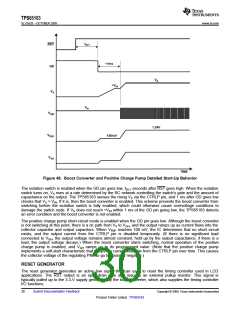
where tDLY is defined by the capacitor connected to the DLY pin. The resulting power-supply sequencing is
shown in Figure 50.
TPS65163
10 kW
ENABLE
CRST
Figure 49. Using an ENABLE Signal to Control Boost Converter and Charge Pumps
VIN > VUVLO
VIN
VLOGIC > VPG
VLOGIC
ENABLE
RST
VGL
tDLY
VGH
VS
Figure 50. Power-Supply Sequencing Using an ENABLE Signal
Copyright © 2009, Texas Instruments Incorporated
Submit Documentation Feedback
31
Product Folder Link(s) :TPS65163

 TI [ TEXAS INSTRUMENTS ]